Download
1 / 51
510 likes | 686 Vues
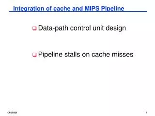
MIPS Pipeline. See P&H Chapter 4.6. A Processor. Review: Single cycle processor. memory. register file. inst. alu. +4. +4. addr. =?. PC. d in. d out. control. cmp. offset. memory. new pc. target. imm. extend. Review: Single Cycle Processor. Advantages

E N D
MIPS Pipeline See P&H Chapter 4.6
A Processor Review: Single cycle processor memory registerfile inst alu +4 +4 addr =? PC din dout control cmp offset memory new pc target imm extend
Review: Single Cycle Processor • Advantages • Single Cycle per instruction make logic and clock simple • Disadvantages • Since instructions take different time to finish, memory and functional unit are not efficiently utilized. • Cycle time is the longest delay. • Load instruction • Best possible CPI is 1
Single Cycle vs Pipelined Processor See: P&H Chapter 4.5
The Kids • Alice • Bob • They don’t always get along…
The Materials Saw Drill Glue Paint
The Instructions • N pieces, each built following same sequence: Saw Drill Glue Paint
Design 1: Sequential Schedule • Alice owns the room • Bob can enter when Alice is finished • Repeat for remaining tasks • No possibility for conflicts
Sequential Performance time1 2 3 4 5 6 7 8 … • Elapsed Time for Alice: 4 • Elapsed Time for Bob: 4 • Total elapsed time: 4*N • Can we do better? Latency: Throughput: Concurrency:
Design 2: Pipelined Design • Partition room into stagesof a pipeline Dave Carol Bob Alice One person owns a stage at a time 4 stages 4 people working simultaneously Everyone moves right in lockstep
Pipelined Performance time1 2 3 4 5 6 7… Latency: Throughput: Concurrency: What if some tasks don’t need drill?
Lessons • Principle: • Throughput increased by parallel execution • Pipelining: • Identify pipeline stages • Isolate stages from each other • Resolve pipeline hazards (Thursday)
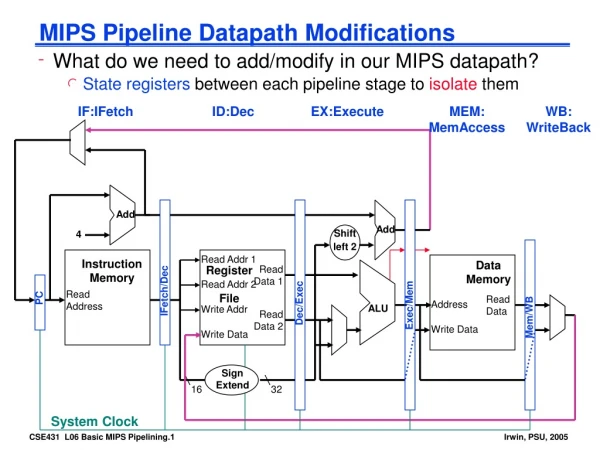
A Processor Review: Single cycle processor memory registerfile inst alu +4 +4 addr =? PC din dout control cmp offset memory new pc target imm extend
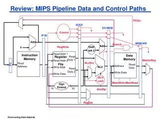
A Processor memory registerfile inst alu +4 addr PC din dout control memory new pc computejump/branchtargets imm extend Write-Back InstructionDecode InstructionFetch Memory Execute
Basic Pipeline Five stage “RISC” load-store architecture • Instruction fetch (IF) • get instruction from memory, increment PC • Instruction Decode (ID) • translate opcode into control signals and read registers • Execute (EX) • perform ALU operation, compute jump/branch targets • Memory (MEM) • access memory if needed • Writeback (WB) • update register file
Time Graphs Clock cycle IF ID EX MEM WB IF ID EX MEM WB IF ID EX MEM WB IF ID EX MEM WB IF ID EX MEM WB Latency: Throughput: Concurrency:
Principles of Pipelined Implementation • Break instructions across multiple clock cycles (five, in this case) • Design a separate stage for the execution performed during each clock cycle • Add pipeline registers (flip-flops) to isolate signals between different stages
Pipelined Processor See: P&H Chapter 4.6
Pipelined Processor memory registerfile A alu D D B +4 addr PC din dout B M inst control memory computejump/branchtargets newpc extend imm Write-Back InstructionDecode InstructionFetch ctrl ctrl ctrl Memory Execute IF/ID ID/EX EX/MEM MEM/WB
IF • Stage 1: Instruction Fetch • Fetch a new instruction every cycle • Current PC is index to instruction memory • Increment the PC at end of cycle (assume no branches for now) • Write values of interest to pipeline register (IF/ID) • Instruction bits (for later decoding) • PC+4 (for later computing branch targets) • Anything needed by later pipeline stages • Next stage will read this pipeline register
IF instructionmemory 1 WE addr mc inst 00 = read word +4 Rest of pipeline PC+4 1 PC pcreg newpc pcrel pcabs pcsel IF/ID
ID • Stage 2: Instruction Decode • On every cycle: • Read IF/ID pipeline register to get instruction bits • Decode instruction, generate control signals • Read from register file • Write values of interest to pipeline register (ID/EX) • Control information, Rd index, immediates, offsets, … • Contents of Ra, Rb • PC+4 (for computing branch targets later)
result ID dest registerfile WE A A Rd D B B Rb Ra decode inst Stage 1: Instruction Fetch Rest of pipeline imm extend PC+4 PC+4 ctrl IF/ID ID/EX
EX • Stage 3: Execute • On every cycle: • Read ID/EX pipeline register to get values and control bits • Perform ALU operation • Compute targets (PC+4+offset, etc.) in case this is a branch • Decide if jump/branch should be taken • Write values of interest to pipeline register (EX/MEM) • Control information, Rd index, … • Result of ALU operation • Value in case this is a memory store instruction
EX pcsel branch? pcreg A D alu B imm B Stage 2: Instruction Decode Rest of pipeline j pcrel + PC+4 target pcabs || ctrl ctrl ID/EX EX/MEM
MEM • Stage 4: Memory • On every cycle: • Read EX/MEM pipeline register to get values and control bits • Perform memory load/store if needed • address is ALU result • Write values of interest to pipeline register (MEM/WB) • Control information, Rd index, … • Result of memory operation • Pass result of ALU operation
MEM pcsel branch? pcreg D D addr B M din dout Stage 3: Execute Rest of pipeline memory pcrel target mc pcabs ctrl ctrl EX/MEM MEM/WB
WB • Stage 5: Write-back • On every cycle: • Read MEM/WB pipeline register to get values and control bits • Select value and write to register file
WB result D M Stage 4: Memory dest ctrl MEM/WB
instmem A A Rd D D D B B inst addr Rb Ra B M dout din imm +4 mem PC+4 PC+4 PC Rd Rd Rd OP OP OP ID/EX EX/MEM MEM/WB IF/ID
Administrivia • HW2 due today • Fill out Survey online. Receive credit/points on homework for survey. • Survey is anonymous Project1 (PA1) due week after prelim • Continue working diligently. Use design doc momentum • Save your work! • Save often. Verify file is non-zero. Periodically save to Dropbox, email. • Beware of MacOSX 10.5 (leopard) and 10.6 (snow-leopard) • Use your resources • Lab Section, Piazza.com, Office Hours, Homework Help Session, • Class notes, book, Sections, CSUGLab
Administrivia • Prelim1:next Tuesday, February 28thin evening • We will start at 7:30pm sharp, so come early • Prelim Review: This Wed / Fri, 3:30-5:30pm, in 155 Olin • Closed Book • Cannot use electronic device or outside material • Practice prelims are online in CMS • Material covered everything up to end of this week • Appendix C (logic, gates, FSMs, memory, ALUs) • Chapter 4 (pipelined [and non-pipeline] MIPS processor with hazards) • Chapters 2 (Numbers / Arithmetic, simple MIPS instructions) • Chapter 1 (Performance) • HW1, HW2, Lab0, Lab1, Lab2
Administrivia Check online syllabus/schedule • http://www.cs.cornell.edu/Courses/CS3410/2012sp/schedule.html • Slides and Reading for lectures • Office Hours • Homework and Programming Assignments • Prelims (in evenings): • Tuesday, February 28th • Thursday, March 29th • Thursday, April 26th Schedule is subject to change
Collaboration, Late, Re-grading Policies • “Black Board” Collaboration Policy • Can discuss approach together on a “black board” • Leave and write up solution independently • Do not copy solutions Late Policy • Each person has a total of four “slip days” • Max of two slip days for any individual assignment • Slip days deducted first for any late assignment, cannot selectively apply slip days • For projects, slip days are deducted from all partners • 20% deducted per day late after slip days are exhausted Regrade policy • Submit written request to lead TA, and lead TA will pick a different grader • Submit another written request, lead TA will regrade directly • Submit yet another written request for professor to regrade.
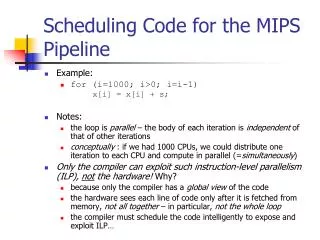
Example: Sample Code (Simple) • Assume eight-register machine • Run the following code on a pipelined datapath add 31 2 ; reg3 = reg 1 + reg 2 nand64 5 ; reg6 = ~(reg 4 & reg 5) lw420 (2) ; reg4 = Mem[reg2+20] add 52 5 ; reg5 = reg 2 + reg 5 sw 7 12(3) ; Mem[reg3+12] = reg 7 Slides thanks to Sally McKee
Example: : Sample Code (Simple) • add r3, r1, r2; nand r6, r4, r5; lw r4, 20(r2); add r5, r2, r5; sw r7, 12(r3);
Time Graphs Clock cycle IF ID EX MEM WB IF ID EX MEM WB IF ID EX MEM WB IF ID EX MEM WB IF ID EX MEM WB Latency: Throughput: Concurrency:
sw r7, 12(r3) sw r7, 12(r3) add r5, r2, r5 sw r7, 12(r3) add r5, r2, r5 lw r4, 20(r2) sw r7, 12(r3) add r5, r2, r5 lw r4, 20(r2) nand r6, r4, r5 sw r7, 12(r3) add r5, r2, r5 lw r4, 20(r2) nand r6, r4, r5 add r3, r1, r2 add r5, r2, r5 lw r4, 20(r2) nand r6, r4, r5 add r3, r1, r2 lw r4, 20(r2) nand r6, r4, r5 add r3, r1, r2 nand r6, r4, r5 add r3, r1, r2 add r3, r1, r2 instmem 0:add1:nand2:lw3:add4:sw A A Rd D D D B B inst addr Rb Ra 77 B M dout din imm +4 mem r0r1r2r3r4r5r6r7 0 36 9 12 18 7 41 22 PC+4 PC+4 PC Rd Rd Rd OP OP OP ID/EX EX/MEM MEM/WB IF/ID
+ A L U M U X 4 target PC+4 PC+4 0 R0 R1 regA ALU result R2 Register file regB valA M U X PC Inst mem Data mem instruction R3 ALU result mdata R4 valB R5 R6 M U X data R7 imm dest extend valB Bits 11-15 Rd dest dest Bits 16-20 M U X Rt Bits 26-31 op op op ID/EX EX/MEM MEM/WB IF/ID
+ A L U M U X 4 0 0 0 0 R0 0 36 R1 0 9 R2 Register file 0 M U X PC Inst mem Data mem nop 12 R3 0 0 18 R4 7 0 R5 41 R6 M U X data 22 R7 0 dest extend 0 Initial State Bits 11-15 0 0 0 Bits 16-20 M U X 0 Bits 26-31 nop nop nop ID/EX EX/MEM MEM/WB IF/ID
+ A L U add 3 1 2 M U X 4 0 4 0 0 R0 0 36 R1 0 9 R2 Register file 0 M U X PC Inst mem Data mem add 3 1 2 12 R3 0 0 18 R4 7 0 R5 41 R6 M U X data 22 R7 0 dest extend 0 Fetch: add 3 1 2 Bits 11-15 0 0 0 Bits 16-20 M U X 0 Bits 26-31 nop nop nop ID/EX EX/MEM MEM/WB IF/ID Time: 1
+ A L U nand 6 4 5 add 3 1 2 M U X 4 0 8 4 0 R0 0 36 R1 1 0 9 R2 Register file 2 36 M U X PC Inst mem Data mem nand 6 4 5 12 R3 0 0 18 R4 7 9 R5 41 R6 M U X data 22 R7 3 dest extend 0 Fetch: nand 6 4 5 Bits 11-15 3 0 0 Bits 16-20 M U X 2 Bits 26-31 add nop nop ID/EX EX/MEM MEM/WB IF/ID Time: 2
+ A L U lw 4 20(2) nand 6 4 5 add 3 1 2 M U X 4 4 12 8 0 R0 0 36 R1 4 0 36 9 R2 Register file 5 18 M U X PC Inst mem Data mem lw 4 20(2) 12 R3 45 0 18 R4 9 7 7 R5 41 R6 M U X data 22 R7 6 dest extend 9 Fetch: lw 4 20(2) Bits 11-15 3 3 6 3 0 Bits 16-20 2 M U X 5 Bits 26-31 nand add nop ID/EX EX/MEM MEM/WB IF/ID Time: 3
+ A L U add 5 2 5 lw 4 20(2) nand 6 4 5 add 3 1 2 M U X 4 8 16 12 0 R0 0 36 R1 2 45 18 9 R2 Register file 4 9 M U X PC Inst mem Data mem add 5 2 5 12 R3 -3 0 18 R4 45 7 7 18 R5 41 R6 M U X data 22 R7 20 dest extend 7 Fetch: add 5 2 5 Bits 11-15 6 3 6 0 6 3 Bits 16-20 5 M U X 4 Bits 26-31 lw nand add ID/EX EX/MEM MEM/WB IF/ID Time: 4
+ A L U sw 7 12(3) add 5 2 5 lw 4 20 (2) nand 6 4 5 add 3 1 2 M U X 4 12 20 16 0 R0 0 45 36 R1 2 -3 9 9 R2 Register file 5 9 M U X PC Inst mem Data mem sw 7 12(3) 45 R3 29 0 18 R4 -3 7 7 R5 41 R6 M U X data 22 R7 20 5 dest extend 18 Fetch: sw 7 12(3) Bits 11-15 0 6 3 4 5 4 6 Bits 16-20 4 M U X 5 Bits 26-31 add lw nand ID/EX EX/MEM MEM/WB IF/ID Time: 5
+ A L U sw7 12(3) add 5 2 5 lw 4 20(2) nand 6 4 5 M U X 4 16 20 0 R0 0 -3 36 R1 3 29 9 9 R2 Register file 7 45 M U X PC Inst mem Data mem 45 R3 16 99 18 R4 29 7 7 22 R5 -3 R6 M U X data 22 R7 12 dest extend 7 No more instructions Bits 11-15 5 4 6 5 0 5 4 Bits 16-20 5 M U X 7 Bits 26-31 sw add lw ID/EX EX/MEM MEM/WB IF/ID Time: 6
+ A L U nopnopsw 7 12(3) add 5 2 5 lw 4 20(2) M U X 4 20 0 R0 0 36 R1 16 45 9 R2 Register file M U X PC Inst mem Data mem 45 R3 99 57 0 99 R4 16 7 R5 -3 R6 M U X data 22 R7 12 dest extend 22 No more instructions Bits 11-15 0 5 4 7 7 5 Bits 16-20 7 M U X Bits 26-31 sw add ID/EX EX/MEM MEM/WB IF/ID Time: 7
+ A L U nopnopnopsw7 12(3) add 5 2 5 M U X 4 0 R0 16 36 R1 57 9 R2 Register file M U X PC Inst mem Data mem 45 R3 0 99 22 R4 57 16 R5 -3 R6 M U X data 22 R7 dest 22 extend No more instructions Bits 11-15 5 7 Bits 16-20 M U X Bits 26-31 sw ID/EX EX/MEM MEM/WB IF/ID Time: 8 Slides thanks to Sally McKee
+ A L U nopnopnopnopsw 7 12(3) M U X 4 0 R0 36 R1 9 R2 Register file M U X PC Inst mem Data mem 45 R3 99 R4 16 R5 -3 R6 M U X data 22 R7 dest extend No more instructions Bits 11-15 Bits 16-20 M U X Bits 21-23 ID/EX EX/MEM MEM/WB IF/ID Time: 9