Download
1 / 21
210 likes | 421 Vues
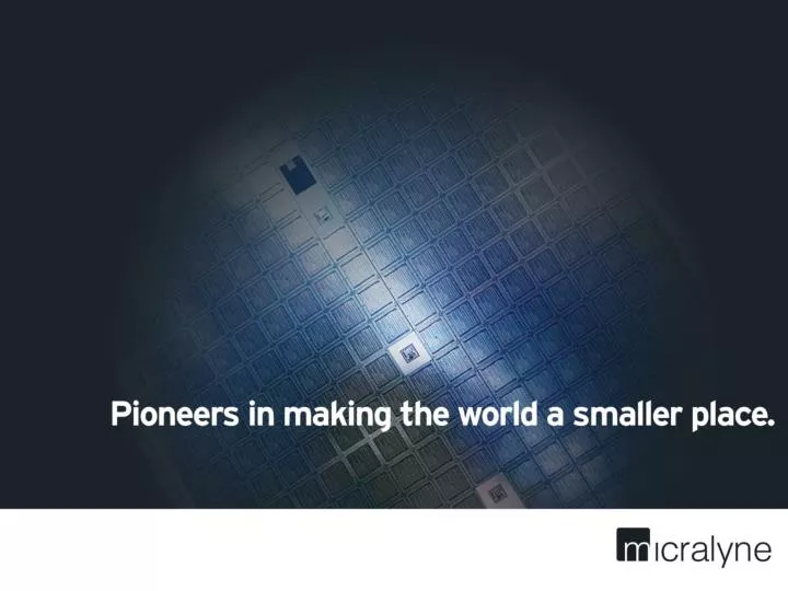
3D Interconnect for MEMS Devices. Collin Twanow Nancy Fares R&D Manager On behalf of President and CEO. About Micralyne. Pure Play MEMS foundry One-stop for Development and Manufacturing Experts in complex 3D MEMS. Contact: info@micralyne.com 780 431 4400 www.micralyne.com.

E N D
3D Interconnect for MEMS Devices Collin Twanow Nancy Fares R&D ManagerOn behalf ofPresident and CEO
About Micralyne • Pure Play MEMS foundry • One-stop for Development and Manufacturing • Experts in complex 3D MEMS Contact: info@micralyne.com 780 431 4400 www.micralyne.com
MEMS – What is it? MEMS – Micro-Electro-Mechanical System • Essentially a devices that interact with its surrounding environment or perform a mechanical function at the micron scale • Think human sensors / structures • Can be built with a IC toolset with the addition of a few specialty tools • A MEMS device is either a • Sensor, or • Actuator, or • Mechanical structure
End Applications and Markets Consumer Off the shelf programmable components for designers. Accelerometers, Gyroscopes, reflector arrays for Display. iPhone orientation sensor, Wii –mote sensor, DLP projectors Defense and Aerospace Self-sustained high precision IMU integrated into equipment—Disposable and extremely accurate Industrial/Structural Self-sustained sensors for strain or seismic sensing on buildings, bridges, etc. Life Sciences Implantable drug devices—Smaller, less intrusive healthcare
MEMS Example Airbag Accelerometer Digital Light Processing TM Technology Courtesy: Texas Instruments
Micralyne MEMS Example – NASA LCROSS NASA mission to determine if water existed at the southern pole of the moon. Crash a rocket stage into a crater, followed by a vehicle sensing material from the ejection plume. Micralyne provided MEMS processing on the detection element of the NIR spectrometer that detected 5.6% water in the crater. (Oct. 2009)
MEMS Compared to ICs Similarities: • Wafer fabrication with common materials and fabrication methods • Silicon wafers, dielectrics, metals • Thin film deposition, photolithography • Market desires increased functionality, reduced size and cost Differences: • Packaging considerations • Fragile mechanical structures • Many MEMS must have access to the surrounding environment • Micron level minimum critical dimensions for mechanical structures • Many device types, fabrication methods, and unique packages
3D Integration – the “Fusion Era” “We are at the doorstep of the largest shift in the semiconductor industry ever, one that will dwarf the PC and even the consumer electronics eras. The core element needed to usher in the new age will be a complex integration of different types of devices such as memory, logic, sensor, processor and software, together with new materials, and advanced die stack technologies, … all based on 3D silicon technology.” Dr. Chang-Gyu Hwang Former President and CEO Samsung Semiconductor IEDM Conf., Dec. 2006
3D IC – MEMS integration Processor IC Integration Memory Analog RF Energy Harvester Inertial Measurement Unit MEMS Strain Gauge Humidity Sensor MEMS MEMS MEMS “Smart Cores” • Dedicated information processing • Each “Smart Core” will process information on its own • Richer data collection • Extended capabilities • Reduce performance requirements across the system • Lower power requirements with specialized processors • Self-sustaining “Smart sensors” • Upgrades are “Plug and play” • Custom, scalable solutions • Combined and sold as a complete system solution MEMS MEMS Thermal Imager CPU MEMS microphone NIR Spectrometer RF MEMS
3D IC a threat? …. Not at all Complimentary Goals Similar challenges P. Leduc CEA Leti 2007
Technology Challenges in 3D Stacking Via Technology: • Via material • Cu, W, or poly-Si • Via process flow • via first, via mid-process, or via last Bonding Technology: • Component arrangement • wafer-to-wafer, wafer-to-chip, or chip-to-chip • Bond-type • Direct bonding, metallic bonding (Cu, CuSn, Au, AuSn), or glue bonding • Bond alignment scheme • face-to-face or face-to-back
Via Materials Cu Via: Poly-Si Via: P. Morrow et al., Intel, AMC 2004 Why poly-Si? • Good for high T processing • Good for high voltage, low current applications • Process compatabiliity Why Cu? • Conductivity • Compatibility with existing metals M. Scannell, CEA-LETI 2007
DeviceLayer DeviceLayer Base Wafer Base Wafer DeviceLayer DeviceLayer DeviceLayer DeviceLayer DeviceLayer DeviceLayer Base Wafer Base Wafer Base Wafer Base Wafer Base Wafer Base Wafer Base Wafer DeviceLayer Base Wafer Base Wafer Base Wafer DeviceLayer DeviceLayer DeviceLayer Via Process Flow Via First: Via Mid-Process: Via Last:
Bonding Component Arrangement Why Chip-to-chip? • Improved final device yields i.e. bonding wafers with random defect densities leads to lower device yield • Incompatible wafer sizes i.e. 12” IC, 6-8” MEMS, 4” InP Why Wafer-to-wafer? • Scalability • Throughput Low Cost
D C B A Key requirements for IC’s • Interconnect reduction • RC delay, Power consumption, Cross talk • Reduce Form Factor • Shielding for Cross talk • Conductive Via Cu, W, Poly-Si P. Leduc CEA Leti 2007 Bonding of devices Multiple stack bonding Compatibility of devices • Cost reduction compared to SoC • Enable new functionalities • Higher Fault resistance • Redundancy Via Density
Addressing the Challenges Integration of bonding and via technologies is a highly constrained problem many aspects of one couple with the other To break these constraints the focus should be upon: Standardization across industry where appropriate i.e. a common Cu-Cu process for one bond in the total integration process is good. Using it for all the bonds necessary to integrate the desired device is bad (last bond ruins all the previous ones) Limiting the impact that the process technology associated with any one device functionality has on the overall complexity of the 3D integration i.e. if MEMS can produce a device that doesn’t constrain the overall thermal budget at all, then that eases the other device constraints
How do MEMS fit? Set boundaries: • Define devices functionality • Understand IC requirements for each – Power, footprint, via density, delay Via specification will define thermal budget and bonding options Revise MEMS process around IC requirements and functionality: • Via Specifications – Conductivity, material, dimension, density 2. Cross talk shielding and requirements • Bonding options during MEMS process • Bonding options for integration.
Next Generation MEMS at Micralyne Micralyne Silicon Platform Bulk Micromachined • Multi layered device Wafer level packaging • Smaller footprint Through-Silicon-Via • Integration (MEMS, IC) Allow room in the packaging / stacking thermal budget for IC integration Cap Wafer TSV DeviceLayer Base Wafer
Currently With 3D IC 3D IC a springboard for MEMS?.. Absolutely • Standardization • Packaging, Integration • With 3D IC • Custom solutions • Smaller devices • Lower cost • Drives innovation in the MEMS Industry • Allows both MEMS and IC companies to focus on core competencies • Device integration without additional design. Ie.) MEMS devices can use off the shelf analog components.
Summary • 3D IC is not a threat – it’s an opportunity for further integration • Major challenges ahead • TSV • Bonding • Standardization • 3D IC and MEMS Integration is the future • Smaller, smarter, feature rich devices • Sell solutions — not components • Through integration of software, IC, and MEMS significant amount of value can be generated • Level of integration driven by performance, size, and cost trade-offs