Download

1 / 27
310 likes | 535 Vues
Clock Generation. 1/16/12 . Required Materials. Clock Generation. Astable Mulivibrator Inverter-Based Oscillator 555 Timer Circuit. Inverter-Based Oscillator. Delay Per Stage of the Inverter. (395 ps ). (273 pS ).

E N D
Clock Generation 1/16/12
Clock Generation • AstableMulivibrator • Inverter-Based Oscillator • 555 Timer Circuit
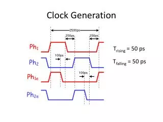
Delay Per Stage of the Inverter (395 ps) (273 pS) Period: 395-273=122 pS, Delay per stage (TD): 234-214=20 pS. Period is 2NTD
Oscillation Frequency Calculation • fosc=2.14 GHz • Tosc=467 pS=2NTD • TD=20 pS • N=Tosc/(2TD)=467 pS/(2 20)=11.68 • N must be odd. • Choose N as 11.
11 Stage Oscillator Period: 1.501 nS-1.052 nS=0.449 nS, Freq=2.227 GHz
555 configured as a monostable circuit + is the pos. of the battery=9V Resistive divider R R R +3 V comparator FF=flip-flip, depicted as a DPDT switch. +6 V - is the neg. term. of the battery=0V (Assumption: pin #3 is connected to 0V)
Comparator We will assume that the FF is in the “up” position when the 555 timer IC is powered up. comparator Each comparator compares two inputs and delivers an output depending on whether the inputs are similar or different. “UP” and “DOWN” remind you what each comparator does when it is activated.
555 configured as a monostable circuit 0 V • Step 1: Ground pin 2, • The output voltage of comparator A goes up • Pin 7 will be disconnected from the ground. • Step 2: • C4 will get charged through R4. • The voltage at pin 6 will go up. 0 V You don’t need to memorize this. Just look at switch drawn in the FF.
555 configured as a monostable circuit Step 3: The voltage at pin 6 will take some time to rise up to 9. Step 4: Note that the voltage at pin 5 is fixed to 2/3 of 9 V. When the voltage at pin 6 exceeds the voltage at pin 5, the output (pin 3) will be grounded and pin 7 will again be connected to ground. (You don’t need to memorize this. Just look at the switch in the flipflop.) 0 V +6V
555 configured as an astable circuit Explanation on the next slide.
Operations of astable timer Let’s assume that C1 is initially grounded. Step 1: A low voltage at pin 2 causes the Comparator to send a “down” signal to FF. Step 2: The output voltage at (pin 3) goes up and the pin 7 is disconnected from R2. (Again, look at the switch in the FF) Step 3: C1 gets charged up through R1+R2. Step 4: The voltage across C1 goes up. Step 5: The voltage at pin 6 exceeds the voltage at pin 5. Step 6: The comparator sends a “high” signal to the flip flop. Step 7: The voltage of Pin 7 goes to ground and The voltage goes to ground. Step 8: C1 discharges through R2. Step 9: Go back to step 1.
Square Wave Oscillator Using 555 Timer IC http://www.falstad.com/circuit/e-555square.html
A Closer Look at the Square Wave Generator http://www.falstad.com/circuit/e-555int.html
Sawtooth Oscillator http://www.falstad.com/circuit/e-555saw.html
Low Duty Cycle http://www.falstad.com/circuit/e-555lowduty.html