Download
1 / 1
10 likes | 129 Vues
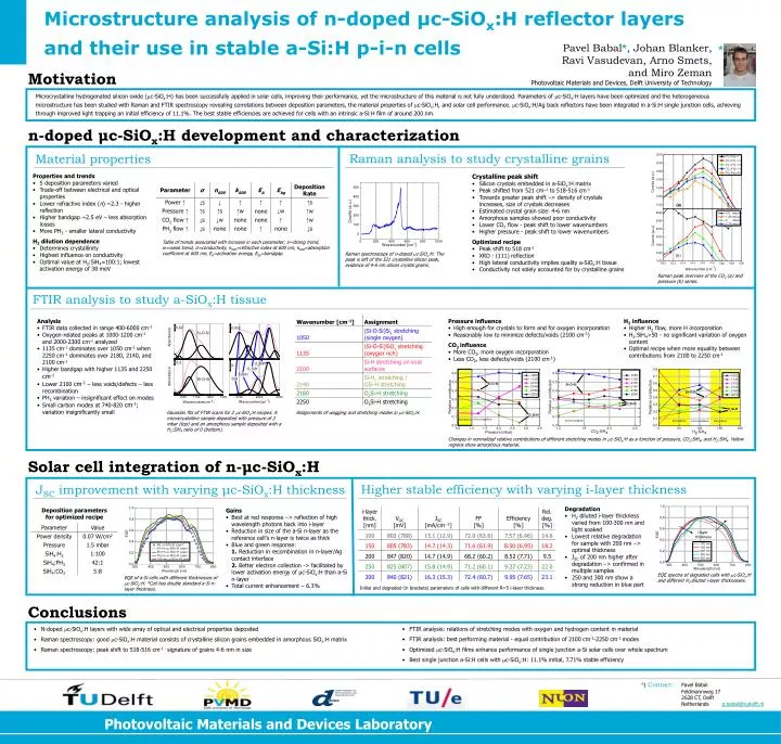
Microstructure analysis of n-doped μ c-SiO x :H reflector layers and their use in stable a-Si:H p-i-n cells. Pavel Babal * , Johan Blanker, Ravi Vasudevan, Arno Smets, and Miro Zeman Photovoltaic Materials and Devices, Delft University of Technology. *. Motivation.

E N D
Microstructure analysis of n-doped μc-SiOx:H reflector layers and their use in stable a-Si:H p-i-n cells Pavel Babal*, Johan Blanker, Ravi Vasudevan, Arno Smets, and Miro ZemanPhotovoltaic Materials and Devices, Delft University of Technology * Motivation Microcrystalline hydrogenated silicon oxide (c-SiOx:H) has been successfully applied in solar cells, improving their performance, yet the microstructure of this material is not fully understood. Parameters of c-SiOx:H layers have been optimized and the heterogeneous microstructure has been studied with Raman and FTIR spectroscopy revealing correlations between deposition parameters, the material properties of c-SiOx:H, and solar cell performance. c-SiOx:H/Ag back reflectors have been integrated in a-Si:H single junction cells, achieving through improved light trapping an initial efficiency of 11.1%. The best stable efficiencies are achieved for cells with an intrinsic a-Si:H film of around 200 nm. n-doped μc-SiOx:H development and characterization Raman analysis to study crystalline grains Material properties • Properties and trends • 5 deposition parameters varied • Trade-off between electrical and optical properties • Lower refractive index (n) ~2.3 - higher reflection • Higher bandgap ~2.5 eV – less absorption losses • More PH3 - smaller lateral conductivity • H2 dilution dependence • Determines crystallinity • Highest influence on conductivity • Optimal value at H2:SiH4=100:1; lowest activation energy of 38 meV • Crystalline peak shift • Silicon crystals embedded in a-SiOx:H matrix • Peak shifted from 521 cm-1 to 518-516 cm-1 • Towards greater peak shift –> density of crystals increases, size of crystals decreases • Estimated crystal grain size: 4-6 nm • Amorphous samples showed poor conductivity • Lower CO2 flow - peak shift to lower wavenumbers • Higher pressure - peak shift to lower wavenumbers • Optimized recipe • Peak shift to 518 cm-1 • XRD - (111) reflection • High lateral conductivity implies quality a-SiOx:H tissue • Conductivity not solely accounted for by crystalline grains Table of trends associated with increase in each parameter; s=strong trend, w=weak trend, σ=conductivity, n600=refractive index at 600 nm, k600=absorption coefficient at 600 nm, EA=activation energy, Ebg=bandgap. Raman spectroscopy of n-doped c-SiOx:H. The peak is left of the 521 crystalline silicon peak, evidence of 4-6 nm silicon crystal grains. Raman peak overview of the CO2 (a) and pressure (b) series. FTIR analysis to study a-SiOx:H tissue • Analysis • FTIR data collected in range 400-6000 cm-1 • Oxygen-related peaks at 1000-1200 cm-1 and 2000-2300 cm-1 analyzed • 1135 cm-1 dominates over 1050 cm-1 when 2250 cm-1 dominates over 2180, 2140, and 2100 cm-1 • Higher bandgap with higher 1135 and 2250 cm-1 • Lower 2100 cm-1 – less voids/defects – less recombination • PH3 variation – insignificant effect on modes • Small carbon modes at 740-820 cm-1; variation insignificantly small • Pressure influence • High enough for crystals to form and for oxygen incorporation • Reasonably low to minimize defects/voids (2100 cm-1) • CO2 influence • More CO2, more oxygen incorporation • Less CO2, less defects/voids (2100 cm-1) • H2 influence • Higher H2 flow, more H incorporation • H2:SiH4>50 - no significant variation of oxygen content • Optimal recipe when more equality between contributions from 2100 to 2250 cm-1 Gaussian fits of FTIR scans for 2 c-SiOx:H recipes. A microcrystalline sample deposited with pressure of 2 mbar (top) and an amorphous sample deposited with a H2:SiH4 ratio of 0 (bottom). Assignments of wagging and stretching modes in c-SiOx:H. Changes in normalized relative contributions of different stretching modes in c-SiOx:H as a function of pressure, CO2:SiH4, and H2:SiH4. Yellow regions show amorphous material. Solar cell integration of n-μc-SiOx:H Higher stable efficiency with varying i-layer thickness JSC improvement with varying μc-SiOx:H thickness • Degradation • H2 diluted i-layer thickness varied from 100-300 nm and light soaked • Lowest relative degradation for sample with 200 nm –> optimal thickness • JSC of 200 nm higher after degradation –> confirmed in multiple samples • 250 and 300 nm show a strong reduction in blue part Deposition parameters for optimized recipe • Gains • Best at red response –> reflection of high wavelength photons back into i-layer • Reduction in size of the a-Si n-layer as the reference cell's n-layer is twice as thick • Blue and green response: • 1. Reduction in recombination in n-layer/Ag contact interface • 2. Better electron collection -> facilitated by lower activation energy of μc-SiOx:H than a-Si n-layer • Total current enhancement – 6.3% EQE spectra of degraded cells with c-SiOx:H and different H2 diluted i-layer thicknesses. EQE of a-Si cells with different thicknesses of c-SiOx:H. *Cell has double standard a-Si n-layer thickness. Initial and degraded (in brackets) parameters of cells with different R=5 i-layer thickness. Conclusions • FTIR analysis: relations of stretching modes with oxygen and hydrogen content in material • FTIR analysis: best performing material - equal contribution of 2100 cm-1-2250 cm-1 modes • Optimized c-SiOx:H films enhance performance of single junction a-Si solar cells over whole spectrum • Best single junction a-Si:H cells with c-SiOx:H: 11.1% initial, 7.71% stable efficiency • N-doped c-SiOx:H layers with wide array of optical and electrical properties deposited • Raman spectroscopy: good c-SiOx:H material consists of crystalline silicon grains embedded in amorphous SiOx:H matrix • Raman spectroscopy: peak shift to 518-516 cm-1 - signature of grains 4-6 nm in size *) Contact:Pavel Babal Feldmannweg 17 2628 CT, Delft Netherlands p.babal@tudelft.nl Photovoltaic Materials and Devices Laboratory