Download
1 / 56
560 likes | 569 Vues
Chapter 2 Interconnect Analysis Delay Modeling. Prof. Lei He Electrical Engineering Department University of California, Los Angeles URL: eda.ee.ucla.edu Email: lhe@ee.ucla.edu. Outline. Delay models RC tree Elmore delay Gate delay Homework 2. Input-to-Output Propagation Delay.

E N D
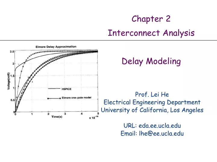
Chapter 2Interconnect AnalysisDelay Modeling Prof. Lei He Electrical Engineering Department University of California, Los Angeles URL: eda.ee.ucla.edu Email: lhe@ee.ucla.edu
Outline • Delay models • RC tree Elmore delay • Gate delay • Homework 2
Input-to-Output Propagation Delay • The circuit delay in VLSI circuits consists of two components: • The 50% propagation delay of the driving gates (known as the gate delay) • The delay of electrical signals through the wires (known as the interconnect delay)
R r r r r c c c c C Lumped vs Distributed Interconnect Model Lumped Distributed How to analyze the delay for each model?
R u(t) v(t) C Lumped RC Model Impulse response and step response of a lumped RC circuit
v0 v0 R v0(1-eRC/T) C Analysis of Lumped RC Model S-domain ckt equation (current equation) Frequency domain response for step-input Frequency domain response for impulse match initial state: Time domain response for step-input: Time domain response for impulse:
1v V(t) R C 50% Delay for lumped RC model 1 0.5 50% delay How about more complex circuits?
2 R4 R2 C4 C2 R1 4 1 s R3 Ri Ci C1 3 C3 i Distributed RC-Tree • The network has a single input node • All capacitors between node and ground • The network does not contain any resistive loop
2 R4 R2 C4 C2 R1 4 1 s R3 Ri Ci C1 3 C3 i RC-tree Property • Unique resistive path between the source node s and any other node i of the network path resistance Rii • Example: R44=R1+R3+R4
2 R4 R2 C4 C2 R1 4 1 s R3 Ri Ci C1 3 C3 i RC-tree Property • Extended to shared path resistance Rik: Example: Ri4=R1+R3 Ri2=R1
Elmore Delay • Assuming: • Each node is initially discharged to ground • A step input is applied at time t=0 at node s • The Elmore delay at node i is: • Theorem: The Elmore delay is equivalent to the first-order time constant of the network • Proven acceptable approximation of the real delay • Powerful mechanism for a quick estimate
2 R4 R2 C4 C2 R1 4 1 s R3 Ri Ci C1 3 C3 i Example • Elmore delay at node i is
Definition h(t) = impulse response TD = mean of h(t) = Interpretation H(t) = output response (step process) h(t) = rate of change of H(t) T50%= median of h(t) Elmore delay approximates the median of h(t) by the mean of h(t) h(t) = impulse response H(t) = step response median of h(t) (T50%) Interpretation of Elmore Delay
R1 R2 RN C1 C2 CN Vin VN RC-chain (or ladder) • Special case: • Shared-path resistance path resistance
R R R C C C RC-Chain Delay VN Vin R=r · L/N C=c·L/N • Delay of wire is quadratic function of its length • Delay of distributed rc-line is half of lumped RC
Outline • Delay models • RC tree Elmore delay • Gate delay
Gate Delay and Output Transition Time • The gate delay and the output transition time are functions of both input slew and the output load
Output Transition Time Vout Vin W W p p 90% Vin Vout C C t M M out Cdiff Cload W W t t t 10% n n in in out Time Cout Gate Delay Definitions
Output Transition time (s) Output Transition time (s) 10-14 CLoad (F) 10-10 Input Transition Time (s) Output Transition Time • Output transition time as a function of input transition time and output load
ASIC Cell Delay Model • Three approaches for gate propagation delay computation are based on: • Delay look-up tables • K-factor approximation • Effective capacitance • Delay look-up table is currently in wide use especially in the ASIC design flow • Effective capacitance promises to be more accurate when the load is not purely capacitive
115pS Table Look-Up Method • What is the delay when Cloadis 505f F and Tin is 90pS?
Output Transition time (s) Output Transition time (s) 10-14 CLoad (F) Input Transition Time (s) 10-10 K-factor Approximation • We can fit the output transition time v.s. input transition time and output load as a polynomial function, e.g. • A similar equation gives the gate delay
One Dimensional Table Linear model
D2 D1 D3 D4 Two Dimensional Table Quadratic model
Second-order RC-p Model • Using Taylor Expansion around s = 0
Second-order RC-p Model (Cont’d) • This equation requires creation of a four-dimensional table to achieve high accuracy • This is however costly in terms of memory space and computational requirements
Effective Capacitance Approach • The “Effective Capacitance” approach attempts to find a single capacitance value that can be replaced instead of the RC-p load such that both circuits behave similarly during transition
Rp 0 k = 1 Rp ∞ k = 0 Effective Capacitance (Cont’d) 0<k<1 • Because of the shielding effect of the interconnect resistance , the driver will only “see” a portion of the far-end capacitance C2
Macy’s Approach • Assumption: If two circuits have the same loads and output transition times, then their effective capacitances are the same • => the effective capacitance is only a function of the output transition time and the load
Macy’s Iterative Solution • Compute a from C1 and C2 • Choose an initial value for Ceff • Compute Tout for the given Ceff and Tin • Compute b • Compute g from a and b • Find new Ceff • Go to step 3 until Ceffconverges
Summary • Delay model • Elmore delay • Gate delay: look-up table, k-factor approximation, effective capacitance 37
References • R. Macys and S. McCormick, “A New Algorithm for Computing the “Effective Capacitance” in Deep Sub-micron Circuits”, Custom Integrated Circuits Conference 1998, pp. 313-316 • J. Cong, Z. Pan and P. V. Srinivas, "Improved Crosstalk Modeling for Noise Constrained Interconnect Optimization", Asia and South Pacific Design Automation Conference 2001, pp. 373-378 • L. H. Chen, M. M.-Sadowska, “Aggressor Alignment for Worst-case Coupling Noise”, International Symposium on Physical Design 2000, pp. 48-54 38
[1] Given the circuit as shown below and a unit step voltage source at the input node s, use SPICE to simulate the circuit and obtain the accurate 50% delay at node n. Also analytically calculate the delay using Elmore method and S2P method. How do they compare with the result obtained by SPICE? Homework R4 R2 C4 C2 R1 s R3 R5 C5 C1 n 1v C3 R1 = 1mΩ R2 = 2mΩ R3 = 2mΩ R4 = 1mΩ R5 = 4mΩ C1 = 1nF C2 = 1nF C3 = 4nF C4 = 4nF C5 = 2nF
R4 R2 C4 C2 R1 s R3 C6 C5 C1 n 1v C3 Homework [2] Give the circuit as shown below and a unit step voltage source at node s, can we still use the “shared-path” formula to calculate the Elmore delay? Explain why or why not. Use DC analysis method via MATLAB or SPICE to get the 0th -3rd moments of C3 and C5. R1 = 1mΩ R2 = 2mΩ R3 = 2mΩ R4 = 1mΩ C1 = 1nF C2 = 1nF C3 = 4nF C4 = 4nF C5 = 2nF C6 = 1nF 40
Steps for Problem 1 1. Write the SPICE netlist of the circuit and probe the voltage response at node n. 2. Record the time when the voltage at node n reaches 0.5V. That time is the 50% delay. 3. Use the Elmore delay formula to calculate the Elmore delay. (find the shared path between each node and node n). 4. Write down the transfer function and driving point admittance of the circuit with input s and output n. 5. Expand the transfer function to get the moments m1* and m2*. Expand the driving point admittance to get m1, m2, m3, and m4. 41
Steps for Problem 1 6. Follow the S2P algorithm to get k1, k2, p1 and p2. 7. Use the frequency domain expression (h(s)) to derive the time domain expression (h(t)). 8. Plot the obtained time domain waveform to get the 50% delay for the S2P model. 9. Compare the results. 42
Steps for Problem 2 1. Follow the DC analysis method to reconstruct the circuit (e.g. replace C with zero current source for 0th moment calculation, etc). 2. Stamp the G and C matrices for MATLAB analysis or write the corresponding netlist for SPICE analysis. 3. Get the voltage across the capacitance as the moment. 4. The above should be done repeatedly until all the desired moments are acquired. 43
Homework 2 [3] Modify the PRIMA code with single frequency expansion to multiple points expansion. You should use a vector fspan to pass the frequency expansion points. Compare the waveforms of the reduced model between the following two cases: 1. Single point expansion at s=1e4. 2. Four-point expansion at s=1e3, 1e5, 1e7, 1e9. 44
Format of the input matrices for test 1 1 19.4595 1.43391e-14 1 2 0.000464141 -2.9702e-15 1 3 -0.000542882 0.0 1 4 0.000152585 -7.5288e-15 1 5 0.000464074 -2.9702e-15 1 6 -0.000542801 0.0 1 68 -19.4595 0.0 2 1 0.0 -2.9702e-15 2 2 3.66672 2.44291e-13 2 3 0.0 -2.3594e-13 2 4 0.0 -5.3806e-15 2 72 -1.425 0.0 2 329 -2.06075 0.0 2 341 -0.091255 0.0 2 343 -0.0897199 0.0 3 1 -2.44188e-06 0.0 3 2 -0.000464141 -2.3594e-13 3 3 40.8898 2.42089e-13 ….. 45