Download
1 / 134
1.88k likes | 2.96k Vues
Chapter 8 Oscillators. 8.1 Performance Parameters 8.2 Basic Principles 8.3 Cross-Coupled Oscillator 8.4 Three-Point Oscillators 8.5 Voltage-Controlled Oscillators 8.6 LC VCOs with Wide Tuning Range 8.7 Phase Noise 8.8 Design Procedure 8.9 LO Interface 8.10 Mathematical Model of VCOs

E N D
Chapter 8 Oscillators • 8.1 Performance Parameters • 8.2 Basic Principles • 8.3 Cross-Coupled Oscillator • 8.4 Three-Point Oscillators • 8.5 Voltage-Controlled Oscillators • 8.6 LC VCOs with Wide Tuning Range • 8.7 Phase Noise • 8.8 Design Procedure • 8.9 LO Interface • 8.10 Mathematical Model of VCOs • 8.11 Quadrature Oscillators • 8.12 Appendix A: Simulation of Quadrature Oscillators Behzad Razavi, RF Microelectronics. Prepared by Bo Wen, UCLA
Chapter Outline • Feedback View • One-Port View • Cross-Coupled Oscillator • Three-Point Oscillators • Tuning Limitations • Effect of Varactor Q • VCOs with Wide Tuning Range General Principles Quadrature VCOs Voltage-Controlled Oscillators Phase Noise • Effect of Phase Noise • Analysis Approach I • Analysis Approach II • Noise of Bias Current • VCO Design Procedure • Low-Noise VCOs • Coupling into an Oscillator • Basic Topology • Properties of Quadrature Oscillators • Improved Topologies
Performance Parameters: Frequency Range • An RF oscillator must be designed such that its frequency can be varied (tuned) across a certain range. This range includes two components: • (1) the system specification; • (2) additional margin to cover process and temperature variations and errors due to modeling inaccuracies. A direct-conversion transceiver is designed for the 2.4-GHz and 5-GHz wireless bands. If a single LO must cover both bands, what is the minimum acceptable tuning range? For the lower band, 4.8 GHz ≤ fLO ≤ 4.96 GHz. Thus, we require a total tuning range of 4.8 GHz to 5.8 GHz, about 20%. Such a wide tuning range is relatively difficult to achieve in LC oscillators.
Performance Parameters: Output Voltage Swing & Drive Capability • The oscillators must produce sufficiently large output swings to ensure nearly complete switching of the transistors in the subsequent stages. • Furthermore, excessively low output swings exacerbate the effect of the internal noise of the oscillator. • In addition to the downconversion mixers, the oscillator must also drive a frequency divider, denoted by a ÷N block.
Performance Parameters: Drive Capability • Typical mixers and dividers exhibit a trade-off between the minimum LO swing with which they can operate properly and the capacitance that they present at their LO port. • We can select large LO swings so that VGS1-VGS2 rapidly reaches a large value, turning off one transistor. • Alternatively, we can employ smaller LO swings but wider transistors so that they steer their current with a smaller differential input. • To alleviate the loading presented by mixers and dividers and perhaps amplify the swings, we can follow the LO with a buffer.
LO Port of Downconversion Mixers and Upconversion Mixers Prove that the LO port of downconversion mixers presents a mostly capacitive impedance whereas that of upconversion mixers also contains a resistive component. Here, Rp represents a physical load resistor in a downconversion mixer, forming a low-pass filter with CL. In an upconversion mixer, on the other hand, Rp models the equivalent parallel resistance of a load inductor at resonance. the input admittance of the circuit and show that the real part reduces to In a downconversion mixer, the -3-dB bandwidth at the output node is commensurate with the channel bandwidth and hence very small. That is, we can assume RpCL is very large, Assume that CL >> CGD in a downconversion mixer In an upconversion mixer, equation above may yield a substantially lower input resistance.
Performance Parameters: Phase Noise & Output Waveform • The spectrum of an oscillator in practice deviates from an impulse and is “broadened” by the noise of its constituent devices, called “phase noise”. • Unfortunately, phase noise bears direct trade-offs with the tuning range and power dissipation of oscillators, making the design more challenging. • Abrupt LO transitions reduce the noise and increase the conversion gain. • Effects such as direct feedthrough are suppressed if the LO signal has a 50% duty cycle. • Sharp transitions also improve the performance of frequency dividers. • Thus, the ideal LO waveform in most cases is a square wave. • In practice, it is difficult to generate square LO waveforms. • A number of considerations call for differential LO waveforms.
Performance Parameters: Supply Sensitivity & Power Dissipation • The frequency of an oscillator may vary with the supply voltage, an undesirable effect because it translates supply noise to frequency (and phase) noise. • The power drained by the LO and its buffer(s) proves critical in some applications as it trades with the phase noise and tuning range.
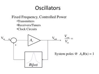
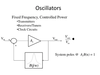
Feedback View of Oscillators • An oscillator may be viewed as a “badly-designed” negative-feedback amplifier—so badly designed that it has a zero or negative phase margin. For the above system to oscillate, must the noise at ω1 appear at the input? No, the noise can be anywhere in the loop. For example, consider the system shown in figure below, where the noise N appears in the feedback path. Here, Thus, if the loop transmission, H1H2H3, approaches -1 at ω1, N is also amplified indefinitely.
Y/X in the Vicinity of ω = ω1 Derive an expression for Y/X in figure below in the vicinity of ω = ω1 if H(jω1) = -1. We can approximate H(jω) by the first two terms in its Taylor series: Since H(jω1) = -1, we have As expected, Y/X → ∞ as Δω → 0, with a “sharpness” proportional to dH/dω.
Barkhausen’s Criteria • For the circuit to reach steady state, the signal returning to A must exactly coincide with the signal that started at A. We call ∠ H(jω1) a “frequency-dependent” phase shift to distinguish it from the 180 ° phase due to negative feedback. • Even though the system was originally configured to have negative feedback, H(s) is so “sluggish” that it contributes an additional phase shift of 180 ° at ω1, thereby creating positive feedback at this frequency.
Significance of |H(jw1)| = 1 • For a noise component at ω1 to “build up” as it circulates around the loop with positive feedback, the loop gain must be at least unity. • We call |H(jω1)| = 1 the “startup” condition. • What happens if |H(jω1)| > 1 and ∠H(jω1) = 180°? The growth shown in figure above still occurs but at a faster rate because the returning waveform is amplified by the loop. • Note that the closed-loop poles now lie in the right half plane.
Can a Two-Pole System Oscillate? (Ⅰ) Can a two-pole system oscillate? Suppose the system exhibits two coincident real poles at ωp. Figure below (left) shows an example, where two cascaded common-source stages constitute H(s) and ωp= (R1C1)-1. This system cannot satisfy both of Barkhausen’s criteria because the phase shift associated with each stage reaches 90° only at ω = ∞, but |H(∞)| = 0. Figure below (right) plots |H| and ∠H as a function of frequency, revealing no frequency at which both conditions are met. Thus, the circuit cannot oscillate.
Can a Two-Pole System Oscillate? (Ⅱ) Can a two-pole system oscillate? But, what if both poles are located at the origin? Realized as two ideal integrators in a loop, such a circuit does oscillate because each integrator contributes a phase shift of -90° at any nonzero frequency. Shown in figure below (right) are |H| and ∠H for this system.
Frequency and Amplitude of Oscillation in Previous Example The feedback loop of figure above is released at t = 0 with initial conditions of z0 and y0 at the outputs of the two integrators and x(t) = 0. Determine the frequency and amplitude of oscillation. Assuming each integrator transfer function is expressed as K/s, Substitute x and y, Interestingly, the circuit automatically finds the frequency at which the loop gain K2/ω2drops to unity.
Ring Oscillator • Other oscillators may begin to oscillate at a frequency at which the loop gain is higher than unity, thereby experiencing an exponential growth in their output amplitude. • The growth eventually stops due to the saturating behavior of the amplifier(s) in the loop. • Each stage operates as an amplifier, leading to an oscillation frequency at which each inverter contributes a frequency-dependent phase shift of 60°.
Example of Voltage Swings (Ⅰ) The inductively-loaded differential pair shown in figure below is driven by a large input sinusoid at Plot the output waveforms and determine the output swing. With large input swings, M1 and M2 experience complete switching in a short transition time, injecting nearly square current waveforms into the tanks. Each drain current waveform has an average of ISS/2 and a peak amplitude of ISS/2. The first harmonic of the current is multiplied by Rp whereas higher harmonics are attenuated by the tank selectivity.
Example of Voltage Swings (Ⅱ) Recall from the Fourier expansion of a square wave of peak amplitude A (with 50% duty cycle) that the first harmonic exhibits a peak amplitude of (4/π)A (slightly greater than A). The peak single-ended output swing therefore yields a peak differential output swing of
One-Port View of Oscillators • An alternative perspective views oscillators as two one-port components, namely, a lossy resonator and an active circuit that cancels the loss. • If an active circuit replenishes the energy lost in each period, then the oscillation can be sustained. • In fact, we predict that an active circuit exhibiting an input resistance of -Rp can be attached across the tank to cancel the effect of Rp.
How Can a Circuit Present a Negative Input Resistance? • The negative resistance varies with frequency.
Connection of Lossy Inductor to Negative-Resistance Circuit • Since the capacitive component in equation above can become part of the tank, we simply connect an inductor to the negative-resistance port. Express the oscillation condition in terms of inductor’s parallel equivalent resistance, Rp, rather than RS. The startup condition:
Tuned Oscillator We wish to build a negative-feedback oscillatory system using “LC-tuned” amplifier stages. At very low frequencies, L1 dominates the load and At the resonance frequency At very high frequencies The phase shift from the input to the output is thus equal to 180° |Vout/Vin| dinimishes ∠(Vout/Vin) approaches +90° |Vout/Vin| is very small and ∠(Vout/Vin) remains around -90°
Cascade of Two Tuned Amplifiers in Feedback Loop Can the circuit above oscillate if its input and output are shorted? No. We recognize that the circuit provides a phase shift of 180 ° with possibly adequate gain (gmRp) at ω0. We simply need to increase the phase shift to 360 °. Assuming that the circuit above (left) oscillates, plot the voltage waveforms at X and Y. Wave form is shown above (right). A unique attribute of inductive loads is that they can provide peak voltages above the supply. The growth of VX and VY ceases when M1 and M2 enter the triode region for part of the period, reducing the loop gain.
Cross-Coupled Oscillator The oscillator above (left) suffers from poorly-defined bias currents. The circuit above (middle) is more robust and can be viewed as an inductively-loaded differential pair with positive feedback. Compute the voltage swings in the circuit above (middle) if M1 and M2 experience complete current switching with abrupt edges.
Above-Supply Swings in Cross-Coupled Oscillator • Each transistor may experience stress under the following conditions: • (1) The drain reaches VDD+Va. The transistor remains off but its drain-gate voltage is equal to 2Va and its drain-source voltage is greater than 2Va. • (2) The drain falls to VDD - Va while the gate rises to VDD + Va. Thus, the gate-drain voltage reaches 2Va and the gate-source voltage exceeds 2Va. • Proper choice of Va, ISS, and device dimensions avoids stressing the transistors.
Example of Supply Sensitivity of Cross-Coupled Oscillator A student claims that the cross-coupled oscillator below exhibits no supply sensitivity if the tail current source is ideal. Is this true? No, it is not. The drain-substrate capacitance of each transistor sustains an average voltage equal to VDD. Thus, supply variations modulate this capacitance and hence the oscillation frequency.
One-Port View of Cross-Coupled Oscillator For gm1 = gm2 =gm For oscillation to occur, the negative resistance must cancel the loss of the tank:
Three-Point Oscillators Three different oscillator topologies can be obtained by grounding each of the transistor terminals. Figures below depict the resulting circuits if the source, the gate, or the drain is (ac) grounded, respectively. If C1 = C2, the transistor must provide sufficient transconductance to satisfy • The circuits above may fail to oscillate if the inductor Q is not very high.
Differential Version of Three-Point Oscillators • Another drawback of the circuits shown above is that they produce only single-ended outputs. It is possible to couple two copies of one oscillator so that they operate differentially. • If chosen properly, the resistor R1 prohibits common-mode oscillation. • Even with differential outputs, the circuit above may be inferior to the cross-coupled oscillator previous discussed —not only for the more stringent start-up condition but also because the noise of I1 and I2 directly corrupts the oscillation.
Voltage-Controlled Oscillators: Characteristic • The output frequency varies from ω1 to ω2 (the required tuning range) as the control voltage, Vcont, goes from V1 to V2. • The slope of the characteristic, KVCO, is called the “gain” or “sensitivity” of the VCO and expressed in rad/Hz/V.
Example: VDD as the “Control Voltage” As explained in previous example, the cross-coupled oscillator exhibits sensitivity to VDD. Considering VDD as the “control voltage,” determine the gain. If C1 includes all circuit capacitances except CDB The junction capacitance is approximated as
VCO Using MOS Varactors • Since it is difficult to vary the inductance electronically, we only vary the capacitance by means of a varactor. • MOS varactors are more commonly used than pn junctions, especially in low-voltage design. • First, the varactors are stressed for part of the period if Vcont is near ground and VX (or VY ) rises significantly above VDD. • Second, only about half of Cmax - Cmin is utilized in the tuning.
Oscillator Using Symmetric Inductor • Symmetric spiral inductors excited by differential waveforms exhibit a higher Q than their single-ended counterparts. The symmetric inductor above has a value of 2 nH and a Q of 10 at 10 GHz. What is the minimum required transconductance of M1 and M2 to guarantee start-up?
Tuning Range Limitations We make a crude approximation, Cvar << C1, and If the varactor capacitance varies from Cvar1 to Cvar2, then the tuning range is given by • The tuning range trades with the overall tank Q. • Another limitation on Cvar2 - Cvar1 arises from the available range for the control voltage of the oscillator, Vcont.
Effect of Varactor Q: Tank Consisting of Lossy Inductor and Capacitor A lossy inductor and a lossy capacitor form a parallel tank. Determine the overall Q in terms of the quality factor of each. The loss of an inductor or a capacitor can be modeled by a parallel resistance (for a narrow frequency range). We therefore construct the tank as shown below, where the inductor and capacitor Q’s are respectively given by: Merging Rp1 and Rp2 yields the overall Q:
Tank Using Lossy Varactor Transforming the series combination of Cvar and Rvar to a parallel combination The Q associated with C1+Cvar is equal to The overall tank Q is therefore given by Equation above can be generalized if the tank consists of an ideal capacitor, C1, and lossy capacitors, C2-Cn, that exhibit a series resistance of R2-Rn, respectively.
LC VCOs with Wide Tuning Range: VCOs with Continuous Tuning • We seek oscillator topologies that allow both positive and negative (average) voltages across the varactors, utilizing almost the entire range from Cmin to Cmax. The CM level is simply given by the gate-source voltage of a diode-connected transistor carrying a current of IDD/2. We select the transistor dimensions such that the CM level is approximately equal to VDD/2. Consequently, as Vcont varies from 0 to VDD, the gate-source voltage of the varactors, VGS,var, goes from +VDD/2 to –VDD/2,
Output CM Dependence on Bias Current The tail or top bias current in the above oscillators is changed by DI. Determine the change in the voltage across the varactors. Each inductor contains a small low-frequency resistance, rs . If ISS changes by ΔI, the output CM level changes by ΔVCM= (ΔI/2)rs, and so does the voltage across each varactor. In the top-biased circuit, on the other hand, a change of ΔI flows through two diode-connected transistors, producing an output CM change of ΔVCM = (ΔI/2)(1/gm). Since 1/gm is typically in the range of a few hundred ohms, the top-biased topology suffers from a much higher varactor voltage modulation. What is the change in the oscillation frequency in the above example? Since a CM change at X and Y is indistinguishable from a change in Vcont, we have
VCO Using Capacitor Coupling to Varactors • In order to avoid varactor modulation due to the noise of the bias current source, we return to the tail-biased topology but employ ac coupling between the varactors and the core so as to allow positive and negative voltages across the varactors. • The principal drawback of the above circuit stems from the parasitics of the coupling capacitors.
VCO Using Capacitor Coupling to Varactors: Parasitic Capacitances to the Substrate • The choice of CS = 10Cmax reduces the capacitance range by 10% but introduces substantial parasitic capacitances at X and Y or at P and Q because integrated capacitors suffer from parasitic capacitances to the substrate. • Cb/CAB typically exceeds 5%.
VCO Using Capacitor Coupling to Varactors: Effect of the Parasitics of CS1 and CS2 • A larger C1 further limits the tuning range. The VCO above is designed for a tuning range of 10% without the series effect of CS and parallel effect of Cb. If CS = 10Cmax, Cmax = 2Cmin, and Cb = 0.05CS, determine the actual tuning range. Without the effects of CS and Cb For this range to reach 10% of the center frequency, we have With the effects of CS and Cb
Fringe Capacitor • Called a “fringe” or “lateral-field” capacitor, this topology incorporates closely-spaced narrow metal lines to maximize the fringe capacitance between them. The capacitance per unit volume is larger than that of the metal sandwich, leading to a smaller parasitic.
VCO Using NMOS and PMOS Cross-Coupled Pairs • The circuit can be viewed as two back-to-back CMOS inverters, except that the sources of the NMOS devices are tied to a tail current, or as a cross-coupled NMOS pair and a cross-coupled PMOS pair sharing the same bias current. • Proper choice of device dimensions and ISS can yield a CM level at X and Y around VDD/2, thereby maximizing the tuning range.
VCO Using NMOS and PMOS Cross-Coupled Pairs: the Voltage Swing Advantage • An important advantage of the above topology over those previous discussed is that it produces twice the voltage swing for a given bias current and inductor design. • The current in each tank swings between +ISS and -ISS whereas in previous topologies it swings between ISS and zero. The output voltage swing is therefore doubled.
VCO Using NMOS and PMOS Cross-Coupled Pairs: Drawbacks • First, for |VGS3|+VGS1+VISS to be equal to VDD, the PMOS transistors must typically be quite wide, contributing significant capacitance and limiting the tuning range. • Second, the noise current of the bias current source modulates the output CM level and hence the capacitance of the varactors, producing frequency and phase noise. A student attempts to remove the noise of the tail current source by simply eliminating it. Explain the pros and cons of such a topology. The circuit indeed avoids frequency modulation due to the tail current noise. Moreover, it saves the voltage headroom associated with the tail current source. However, the circuit is now very sensitive to the supply voltage. For example, a voltage regulator providing VDD may exhibit significant flicker noise, thus modulating the frequency (by modulating the CM level). Furthermore, the bias current of the circuit varies considerably with process and temperature.
Amplitude Variation with Frequency Tuning • In addition to the narrow varactor capacitance range, another factor that limits the useful tuning range is the variation of the oscillation amplitude. • As the capacitance attached to the tank increases, the amplitude tends to decrease. Suppose the tank inductor exhibits only a series resistance, RS Thus, Rp falls in proportion to ω2 as more capacitance is presented to the tank.
Discrete Tuning • In applications where a substantially wider tuning range is necessary, “discrete tuning” may be added to the VCO so as to achieve a capacitance range well beyond Cmax/Cmin of varactors. The lowest frequency is obtained if all of the capacitors are switched in and the varactor is at its maximum value, The highest frequency occurs if the unit capacitors are switched out and the varactor is at its minimum value,
Discrete Tuning: Variation of Fine Tuning Range Consider the characteristics above more carefully. Does the continuous tuning range remain the same across the discrete tuning range? That is, can we say Δωosc1 ≈ Δωosc2? We expect Δωosc1to be greater than Δωosc2because, with nCu switched into the tanks, the varactor sees a larger constant capacitance. In fact, This variation in KVCO proves undesirable in PLL design.
Discrete Tuning: Issue of Ron(Ⅰ) • The on resistance, Ron, of the switches that control the unit capacitors degrades the Q of the tank.
Issue of Ron(Ⅱ): Effect of Switch Parasitic Capacitances Can we simply increase the width of the switch transistors so as to minimize the effect of Ron? • Wider switches introduce a larger capacitance from the bottom plate of the unit capacitors to ground, thereby presenting a substantial capacitance to the tanks when the switches are off. • This trade-off between the Q and the tuning range limits the use of discrete tuning.