Download
1 / 8
80 likes | 119 Vues
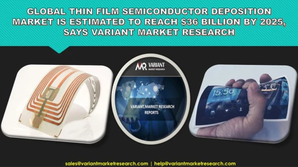
Global Thin Film Semiconductor Deposition Market is estimated to reach $36 billion by 2025; growing at a CAGR of 14.1% from 2017 to 2025.

E N D
Global Thin Film Semiconductor Deposition Market is Estimated to Reach $36 billion by 2025, Says Variant Market Research Dinesh Patel SEO Analyst help@variantmarketresearch.com 1
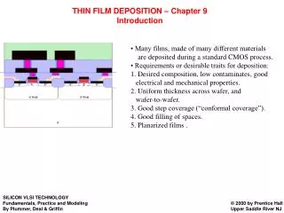
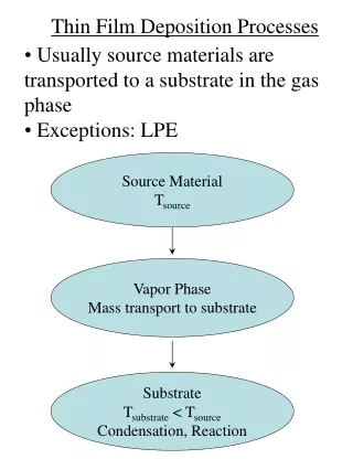
Global Thin Film Semiconductor Deposition Market is estimated to reach $36 billion by 2025; growing at a CAGR of 14.1% from 2017 to 2025.Thin film semiconductors, the foils made from artificial semiconductor materials have the thickness from nanometers to few hundred millimeters. These offer various benefits which includes lightweight, high efficiency, low space consumption, as well as shape flexibility compared to traditional silicon (c-Si). Owing these benefits, the demand for these thin film semiconductors has growing and find widespread applications in DRAMs, solar panels, wearable technologies, and microprocessors, among others. It is used in various industry verticals like IT & telecom, electronics, energy & power, automotive, and aerospace & defense, among others. With increasing demand from various industry verticals, it is expected to boost the growth of the thin film semiconductor deposition market over the forecasted period. Browse categories/semiconductor-electronics/thin-film-semiconductor-deposition-market Complete Report @ https://www.variantmarketresearch.com/report- Global Thin Film Semiconductor Deposition Market Size and Forecast, 2016 - 2025 (US$ Billion) Growing demand for high efficiency & miniaturization, technological advantage of thin film over conventional silicon, increasing demand owing to high usage in emerging applications like dram, flexible OLED displays as well as Amoled displays, and mounting investment in solar power plants are the factors driving the growth of the thin film semiconductor deposition market. However, high investment for manufacturing plant installation may hinder the growth of the market. Moreover, 2
increasing requirement for sensors in smartphone industry might provide with several growth opportunities in the forecasted year. The global thin film semiconductor deposition market is segmented on the basis of technology, industry vertical, and geography. The market is segmented by technology as chemical vapor deposition (CVD), physical vapor deposition (PVD), and others (epitaxy, and electro hydrodynamic deposition). Further, the market is segmented by industry vertical as IT & telecom, electronics, energy & power, automotive, aerospace & defense, and others (healthcare and industrial). Global Thin Film Semiconductor Deposition Market, by Technology Based on geography, global thin film semiconductor deposition market is segmented into North America, Europe, Asia-Pacific, and Rest of the World (RoW). North America is further bifurcated into U.S., Canada, and Mexico whereas Europe segment consist of Germany, France, Italy, and Rest of Europe. Asia-Pacific is segmented into China, Japan, South Korea, Taiwan, India, and Rest of Asia- Pacific while RoW is bifurcated into South America, Middle East, and Africa. Get Sample Report @ https://www.variantmarketresearch.com/report- categories/semiconductor-electronics/thin-film-semiconductor-deposition-market/sample- request The key market players include Hitachi Kokusai Electric Inc., Tokyo Electron Limited, Shin-Etsu Chemical Co., Ltd, Applied Materials, Inc., CVD Equipment Corporation, Lam Research Corporation, 3
AIXTRON SE, Ihi Hauzer Techno Coating B.V, Oerlikon Balzers, and Sumco Corporation, among others. Global Thin Film Semiconductor Deposition market Regional Revenue %(2017 Vs 2025) The key takeaways from the report The key takeaways from the report ❖The report will provide detailed analysis of Global Thin Film Semiconductor Deposition Market with respect to major segments such as technology, and industry vertical ❖The report will include the qualitative and quantitative analysis with market estimation over 2016 – 2025 and compound annual growth rate (CAGR) between 2017 and 2025 ❖Comprehensive analysis of market dynamics including factors and opportunities will be provided in the report ❖An exhaustive regional analysis of Global Thin Film Semiconductor Deposition Market has been included in the report ❖Profile of the key players in the Global Thin Film Semiconductor Deposition Market will be provided, which include key financials, product & services, new developments and business strategies Scope of the Global Thi Scope of the Global Thin Film Semiconductor Deposition Market n Film Semiconductor Deposition Market Technology Segments Chemical Vapor Deposition (CVD) • Physical Vapor Deposition (PVD) • 4
Others (Epitaxy, and Electro Hydrodynamic Deposition) • Industry Vertical Segments IT & Telecom • Electronics • Energy & Power • Automotive • Aerospace & Defense • Others (Healthcare and Industrial) • Geographical Segments North America • oU.S. oCanada oMexico Europe • oGermany oFrance oItaly oRest of Europe Asia-Pacific • oChina oJapan oSouth Korea oTaiwan oIndia oRest of Asia-Pacific RoW • oSouth America oMiddle East oAfrica 5
Global Thin Film Semiconductor Deposition Market Primary Interviews, by Geography Table of Content Chapter 1 Prefix 1.1 Market Scope 1.2 Report Description 1.3 Research Methodology 1.3.1 Primary Research 1.3.2 Secondary Research 1.3.3 In-house Data Modeling Chapter 2 Executive Summary 2.1 Global Thin Film Semiconductor Deposition Market Year-on-Year Growth, 2017 – 2025 (%) Chapter 3 Market Outline 3.1 Market Inclination, Trend, Outlook and Viewpoint 3.2 Market Share Analysis: Company’s Competitive Scenario 3.3 Market Dynamics 3.3.1 Drivers 3.3.1.1 Impact Analysis 6
3.3.2 Restraints 3.3.2.1 Impact Analysis 3.3.3 Opportunities ……………………………. Chapter 7 Company Profiles 7.1 Hitachi Kokusai Electric Inc. 7.2 Tokyo Electron Limited 7.3 Shin-Etsu Chemical Co., Ltd 7.4 Applied Materials, Inc. 7.5 CVD Equipment Corporation 7.6 Lam Research Corporation 7.7 AIXTRON SE 7.8 Ihi Hauzer Techno Coating B.V 7.9 Oerlikon Balzers 7.10 Sumco Corporation About Variant Market Research: Variant Market Research LLP was delineated in 2015 and to launch our business and website it grabbed more than a year. Our head office is based in Pune and we also have branch in San Francisco, California, the U.S. The long time was generally used to build up a talented team of experienced professionals and analysts, to generate client satisfying exact market analysis data. The company aims to be a specialist in delivering reports on various domains with precise analysis, keeping a virtuous relationship with our consumers. Our vision says, "We would like to grow with you, making your paths simpler yet solidest" and our mission is to "Implementing our analytical, technical and marketing skills to set a new goal for our consumers, dedicatedly helping them take their next strategic moves." The Co-founders of Variant Market Research: M/S Shweta Shubham and Mr. Yogesh Godse are keen to provide services across aforementioned domains helping them to take their strategic moves regarding their business and providing them the growth opportunities. The Co-founders say, "We believe in providing the future solutions for your business, exploring the current market trends and suggesting you the future strategies and forecast of a particular market that could keep your company ahead in the competitive market rivalry." We hold expertise in our designated areas of research and consulting with a team of experts from each of the dedicated areas covered under our research. Destined by the dedicated team of analysts and experts, we are envisioned to provide you our best in order to plan your next strategic move and take your company's future ahead with our support and your esteemed cooperation. 7
Contact Us: John Dave, Head – Sales Variant Market Research 649 Mission St, 5th Floor, San Francisco, CA 94105, United States. Tel: +1-415-680-2785 Fax: +1-415-680-2786 Email: john.dave@variantmarketresearch.com Email: help@variantmarketresearch.com 8