Download
1 / 10
100 likes | 260 Vues
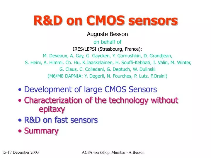
R&D on CMOS sensors. Development of large CMOS Sensors Characterization of the technology without epitaxy R&D on fast sensors Summary. Auguste Besson on behalf of IRES/LEPSI (Strasbourg, France): M. Deveaux, A. Gay, G. Gaycken, Y. Gornushkin, D. Grandjean,

E N D
R&D on CMOS sensors Development of large CMOS Sensors Characterization of the technology without epitaxy R&D on fast sensors Summary Auguste Besson on behalf of IRES/LEPSI (Strasbourg, France): M. Deveaux, A. Gay, G. Gaycken, Y. Gornushkin, D. Grandjean, S. Heini, A. Himmi, Ch. Hu, K.Jaaskelainen, H. Souffi-Kebbati, I. Valin, M. Winter, G. Claus, C. Colledani, G. Deptuch, W. Dulinski (M6/M8 DAPNIA: Y. Degerli, N. Fourches, P. Lutz, F.Orsini) ACFA workshop, Mumbai - A.Besson
Main features of CMOS Sensors P doping • R&D strongly depends on the fabrication technology • Need to explore the different fabrication processes • Key parameters: • Epitaxial layer (≳ 5µm) • Feature size (≲ 0.35µm) • Leakage current • Metalisation(3-5 metal layers) • Etc. Particle path High (p-well) Moderate (Epitaxial layer) High (subtrate) Charge collecting diode Preamplifier (1 in each pixel) Thermal diffusion of electrons 20-40µm Free electron in the conducting band Potential in the diode region • Develop. of large CMOS Sensors • Caracterization of the technology without epitaxy • R&D on fast sensors (SOC) ACFA workshop, Mumbai - A.Besson
Main streams of the R&D • Beam tests at CERN-SPS in 2003 (120 GeV/C -) • M5 (reticle size) • M4 and SUC2 (no epitaxy) • Laboratory tests • M6 (fast data treatment) ACFA workshop, Mumbai - A.Besson
Large CMOS sensors (1) • M1/2 (20 µm pitch) • sp ~ 1.5/2.2 µm with 14/4 µm epitaxial • 1≳ 99% ; 2 ~ 98.5% • Mimosa 5 • AMS 0.6 µm process • Reticle size • 19.4 x 17.4 mm2 • 4 submatrices • 512 x 512 pixels (/each of 4 submatrices) • Performances • 6 wafers (6”) fabricated in 2001 • 3 wafers thinned down to 120 µm • det~ 99% ; sp ~ 2 µm; <gain>~ 0.3 % Mimosa 5 layout ACFA workshop, Mumbai - A.Besson
3-T large CMOS sensors (2) • Beam tests at SPS (2003) • 3 sensors • Performance uniformity tests • Between sub-matrices and sensors • Diode size comparisons Total Charge in N pixels Signal/noise seed pixel Small diode (3x3 µm2) Signal/noise seed pixel Big diode (5x5 µm2) ACFA workshop, Mumbai - A.Besson
Large CMOS sensors (3) • STAR experiment : extension of the Vertex detector (2006) • Charm physics small radius, granular and thin detector • 2 layers of pixels ≳ 1000 cm2 ; Rlayer1 ≳ 2 cm; Rlayer2≲ 4 cm • M5 performances are close to STAR requirements • Started a collaboration with LBL and BNL • What to improve ? • read out time ~ 24 ms < 20 ms • sensor thickness ~ 120 µm ≳ 50 µm • leakage current (because of room T) • yield (not crucial) • First mimo-STAR prototype in summer 2004 (TSMC 0.25 µm tech.) ACFA workshop, Mumbai - A.Besson
No epitaxial layer prototypes • Properties (M4) • AMS 0.35 µm without epitaxial layer • low doping substrate increases µe • 120 GeV/c - SPS beam tests • eff ≳ 99.5% ; sp ~2.5 µm (20 µm pitch) • Application to the European Project for biomedical imaging SUCIMA (SUC2) • beam monitoring and dosimetry • less granularity needed • eff ≳ 99.9% ; sp ~5-6 µm (40 µm pitch) • Submission of Mimosa 9 with AND without epitax. layer in a single AMS 0.35 µm batch (January 2004) M4 Total charge in N pixels M4: Signal/Noise in seed pixel • Fabrication processes with epitaxial layer are not mandatory ! ACFA workshop, Mumbai - A.Besson
R&D on fast sensors (1) • M1-M5 1M pixels read out in 1-10 ms • FLC 1st VD layermust be read out in 25-50 s • potentially tremendous data flow: e.g. 15 bits/pixels, t~25 s 500 Gbits/s/106 pixels! • main goal: fast signal treatment AND data compression integrated in the sensor • Fast // read-out of short columns • Different prototypes with different signal treatment: • M6 (with DAPNIA): tests with 55Fe in 2003, • individual pixels and discri work fine, but large spread of pixel caracteristics (pedestal, noise, gain ?) • M7: available, tests in 2003-04 • M8 (with DAPNIA): submitted in Nov., tests in 2004 (beamstrahlung) ACFA workshop, Mumbai - A.Besson
R&D on fast sensors (2) Mimosa 6 • Mimosa 6 (IRES-LEPSI/DAPNIA) • 0.35 µm MIETEC techno. • 30 columns of 128 pixels r.o. in // • Amplification (5.5) and Correlated Double Sampling integrated in the pixel • 5 MHz effective r.o. freq. • Discriminator (DAPNIA) on chip periphery • Pdiss ~ 500 µW per col. and frame r.o. cycle Charge storage Capacitor (90 fF) 28 µm AC coupling capacitor (50 fF) Distribution of signal amplitude (1pixel) Conversion gain Calib. Peak 5.9 keV ACFA
Summary • Large sensors (M5) (1M pixels, AMS 0.6 m ) • ready to be used for a real detector • 2nd fabrication (23 wafers) with a better yield expected • thinning down to ≲ 50 µm in progress • application to extension of STAR Vertex detector in 2006 • No epitaxial layer sensors (M4, SUC 2) • validated for m.i.p. detection (eff ≳ 99.5%, sp ~2,5 m) • fits industrial CMOS fabrication tendency • Fast response sensors (M6, M7, M8) • studies: fab. techno., charge collection system, signal treatment architecture read out speed, efficiency, zero sup., power diss. etc. • 2003/2004 schedule • Large sensors: M5-B tests yield, achieve thinning • M⋆1 available in summer 2004, tests in autumn • Fast sensors: M7 and M8 tests • M9 (with and without epitaxy) submitted in january 2004 • charge collection studies ionising radiation tol. ACFA workshop, Mumbai - A.Besson