Download
1 / 42
470 likes | 665 Vues
2008 Indium Phosphide and Related Materials Conference, May, Versailles, France. Technology Development & Design for 22 nm InGaAs/InP-channel MOSFETs. M. Rodwell University of California, Santa Barbara. C. Palmstrøm, E. Arkun, P. Simmonds University of Minnesota

E N D
2008 Indium Phosphide and Related Materials Conference, May, Versailles, France Technology Development & Design for 22 nm InGaAs/InP-channel MOSFETs M. RodwellUniversity of California, Santa Barbara C. Palmstrøm, E. Arkun, P. SimmondsUniversity of Minnesota P. McIntyre, J. Harris, Stanford University M. V. Fischetti, C. SachsUniversity of Massachusetts Amherst M. Wistey, U. Singisetti, G. Burek, A. Gossard, S. Stemmer, R. Engel-Herbert, Y. Hwang, Y. Zheng, C. Van de WalleUniversity of California Santa Barbara P. Asbeck, Y. Taur, A. Kummel, B. Yu, D. Wang, Y. Yuan,University of California San Diego rodwell@ece.ucsb.edu 805-893-3244, 805-893-5705 fax
Specific Acknowledgements ( Device Team ) Dr. Mark Wistey Lead: Device DevelopmentMBE Regrowth Uttam Singisetti Prof. Chris PalmstrømCBE Regrowth Greg Burek Dr. Erdem Arkun
Why Develop III-V MOSFETs ? Silicon MOSFETs continue to scale... ...22 nm is feasible in production ( or so the Silicon industry tells us...) ...16 nm ? -- it is not yet clear If we can't make MOSFETs yet smaller,instead move the electrons faster: Id / Wg = qnsv Id / Qtransit = v / Lg III-V materials→ lower m*→ higher velocities Serious challenges: High-K dielectrics on InGaAs channels, InGaAs growth on Si True MOSFET fabrication processes Designing small FETs which use big(low m*) electrons
Goal: double transistor bandwidth when used in any circuit → reduce 2:1 all capacitances and all transport delays→ keep constant all resistances, voltages, currents Simple FET Scaling All lengths, widths, thicknesses reduced 2:1 All lengths, widths, thicknesses reduced 2:1 S/D contact resistivity reduced 4:1 S/D contact resistivity reduced 4:1 If Tox cannot scale with gate length, Cparasitic / Cgs increases, gm / Wg does not increasehence Cparasitic /gm does not scale
FET scaling: Output Conductance & DIBL transconductance output conductance → Keep Lg / Tox constant as we scale Lg
Well-Known: Si FETs No Longer Scale Perfectly Effective oxide thickness is no longer scaling in proportion to Lg (ITRS roadmap copied from Larry Larson's files)
Highly Scaled MOSFETs: What Are Our Goals ? Low off-state current (10 nA/mm) for low static dissipation → minimum subthreshold slope→ minimum Lg / Tox low gate tunneling, low band-band tunneling Low delay CFETDV/I d in gates where transistor capacitances dominate. Parasitic capacitances are 0.5-1.0 fF/mm → while low Cgs is good, high Id is much better Low delay CwireDV/Id in gates where wiring capacitances dominate. large FET footprint → long wires between gates→ need high Id / Wg ; target ~6 mA/mm short transit time alone (low Cgs, intDVgs/DId ) is not sufficient
III-V MOSFETs: Drive Current andCV/I delay
III-V CMOS: The Benefit Is Low Mass, Not High Mobility low effective mass → high currents mobilities above ~ 1000 cm2/V-s of little benefit at 22 nm Lg
Low Effective Mass Impairs Vertical Scaling Shallow electron distribution needed for high gm / Gds ratio, low drain-induced barrier lowering. Energy of Lth well state For thin wells, only 1st state can be populated. For very thin wells, 1st state approaches L-valley. Only one vertical state in well. Mimimum ~ 5 nm well thickness. → Hard to scale below 22 nm Lg.
Density-Of-States Capacitance and n is the # of band minima Two implications: - With Ns >1013/cm2, electrons populate satellite valleys - Transconductance dominated by finite state density Fischetti et al, IEDM2007 Solomon & Laux , IEDM2001
Drive Current in the Ballistic & Degenerate Limits More careful analyses by Taur & Asbeck Groups, UCSD; Fischetti Group: U-Mass: IEDM2007
Drive Current in the Ballistic & Degenerate Limits eot includes the electron wavefunction depth Inclusive of non-parabolic band effects, which increase cdos , InGaAs & InP have near-optimum mass for 0.4-1.0 nm EOT gate dielectrics
Rough Projections From Simple Ballistic Theory 22 nm gate length 0.5-1.0 fF/mm parasitic capacitances Channel EOT drive current intrinsic(700 mV overdrive) gate capacitance InGaAs 1 nm 6 mA/mm 0.2 fF/mm InGaAs 1/2 nm 8.5 mA/mm 0.25 fF/mm Si 1 nm 2.5-3.5 mA/mm 0.7 fF/mm Si 1/2 nm 5-7 mA/mm 1.4 fF/mm InGaAs has much less gate capacitance 1 nm EOT → InGaAs gives much more drive current 1/2 nm EOT → InGaAs & Si have similar drive current InGaAs channel→ no benefit for sub-22-nm gate lengths
Device Structure& Process Flow
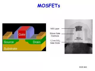
Gate Source Drain Device Fabrication: Goals & Challenges III-V HEMTs are built like this→ K Shinohara ....and most III-V MOSFETs are built like this→
Gate Source Drain Device Fabrication: Goals & Challenges Yet, we are developing,at great effort,a structure like this → Why ? K Shinohara
Gate Source Drain Why not just build HEMTs ? Gate Barrier is Low ! Gate barrier is low: ~0.6 eV K Shinohara Tunneling through barrier→ sets minimum thickness Emission over barrier→ limits 2D carrier density
Gate Source Drain Why not just build HEMTs ? Gate barrier also lies under source / drain contacts N+ layer widegap barrier layer K Shinohara low resistance: need low barrier under contacts low leakage: need high barrier under gate
The Structure We Need -- is Much Like a Si MOSFET no gate barrier under S/D contacts high-K gatebarrier Overlap between gateand N+ source/drain How do we make this device ?
Source/Drain Implantation Does Not Look Easy Implantation will intermix InGaAs well & InAlAs barrier Annealing can't fix this. Incommensurate sublimation of III vs. V elements during anneal Need ~ 5 nm implant depth & ~ 6*1019 /cm3 doping Implanted structures have not shown the necessary low contact resistivity.
So, We Are Forming the Source/Drain By Regrowth Process selected to meet 22 nm ITRS targets But... unlike HEMT process flows,fully established in 1980's... ...most process steps hereare completely new The technology is aggressive and challenging
The Required Performance is Formidable ~5 nm thick well 1 nm Insulator EOT Target ~7 mA/mm @ 700 mV gate overdrive
Gate Dielectrics ALD Al2O3 from IBM (D. Sedana) & Stanford (P. McIntyre) ALD ZrO2 from Intel (S. Koveshnikov et al, DRC 2008) Al2O3 is more robust in processing. → initial process development Process modules being developed for ZrO2 .
Gate Definition: Challenges Must scale to 22 nm Dielectric cap on gate for source/drain regrowth Metal & Dielectric etch must stop in 5 nm channel Semiconductor etch must not etch through 5 nm InP subchannel Process must leave surfaces ready for S/D regrowth
Gate Stack: Multiple Layers & Selective Etches Key: stop etch before reaching dielectric, then gentle low-power etch to stop on dielectric
Sidewall Formation PECVD SiN sidewall deposition, low power anisotropic RIE etch ...sidewall etch must not damage the channel
Clean, Undamaged Surface Before Regrowth undamaged InP subchannel (after Al2O3 dielectric etch & InGaAs recess etch )
Two Source/Drain Regrowth Processes non-selective area S/D regrowth by Molecular Beam Epitaxy: Wistey selective area S/D regrowth by Chemical Beam Epitaxy: Palmstrøm / Arkun
Recess Etch & Regrowth: Inter-Relationships non-selective regrowth selective CBE regrowth or InGaAs/InP composite channel permits selective InGaAs wet-etch, stopping on InP regrowth initiated on InP (desirable ?) If regrowth can extend laterally under sidewall, sidewall can be thicker
Regrowth interface resistance In addition to the contact & link resistances resistance at the regrowth interfaces is also of concern...
Contact & Regrowth Interface Resistance Selective-Arkun Nonselective-Wistey
TEM of Regrowth: InGaAs on InGaAs (Mark Wistey) HRTEM InGaAs n+ regrowth Interface HAADF-STEM` InGaAs n+ Interface 2 nm
Images of MBE Regrowth (dummy sample) Regrowth process is still being de-bugged growth on sidewall: bad ! to suppress, grow hotter lateral regrowth under gate: good ! Oxide TiW
Planarization / Etch-Back Process Ashed-back PR covers S/D contacts Mo etched in SF6/Ar dry etch PR strip removes polymers. Mo protects semiconductor from descum plasma.
Results & Status 1st working devices: (ISCS submission)MBE S/D regrowthincomplete S/D growth under gate→ high access resistance→ low drive current (1 mA/mm !) Cause of Problems related to regrowth on InP subchannelhas impacted both MBE & CBE regrowth ...and is now resolved New devices now in fabrication...stay tuned
InGaAs/InP Channel MOSFETs for VLSI Low-m* materials are beneficial only if EOT cannot scale below ~1/2 nm Devices cannot scale much below 22 nm Lg→ limits IC density Little CV/I benefit in gate lengths below 22 nm Lg Need device structure with very low access resistance radical re-work of device structure & process flow Gate dielectrics, III-V growth on Si: also under intensive development