Download
1 / 12
120 likes | 285 Vues
Status of SOI Pixel Development. July 8, 2009 @Belle II, PXD Mtg. Yasuo Arai (KEK) yasuo.arai@kek.jp http://rd.kek.jp/project/soi/. Multi Project Wafer run schedule SBPIX1 Test Buried p-Well Test. 1. Call for SOI Multi Project Wafer (MPW) run through Facilitation Group. Dear colleagues,

E N D
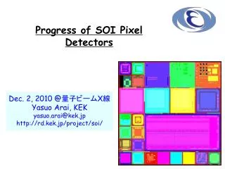
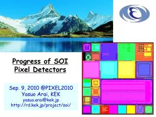
Status of SOI Pixel Development July 8, 2009 @Belle II, PXD Mtg. Yasuo Arai (KEK) yasuo.arai@kek.jp http://rd.kek.jp/project/soi/ • Multi Project Wafer run schedule • SBPIX1 Test • Buried p-Well Test 1
Call for SOI Multi Project Wafer (MPW) runthrough Facilitation Group Dear colleagues, You may know that a facilitation group for monolithic and verticallyintegrated pixel sensors has been established by the three RegionalDirectors (CERN, FNAL and KEK) ... On behalf the facilitation group for monolithic and vertically integratedpixel sensors (Marcel Demarteau, Junji Haba, Hans-Günther Moser and ValerioRe) we would like to announce an offer from KEK to participate in a MPW runwith OKI. ....
FY2009 MPW Schedule *1st MPW: submission on 7th Aug. 2009 *2nd MPW: submission on end. Oct. 2010 *3rdMPW: submission on beg. Jan. 2010 We have received several contacts from foreign labs ; India, UK, Spain, USA, Poland ... Cross Section of Silicon-On-Insulator Pixel
SBPIX1 : First Test Chip for Belle II By Yasuyuki Horii
SBPIX1 First Test chip for Belle II 5 mm x 5 mm
SBPIX1 Pixel Trigger Latency
First Image taken by Laser Light Beam test is under planning. Sum for 3000 events.
p/n Implant and Buried P-Well (BPW) B (~1E12 cm-2) B or P(~5E15cm-2) Buried Oxide SOI Si PSUB BPW • Cut Top Si • High Dose • Keep Top Si • Low Dose
Suppression of Back Gate Effect with BPW Without BPW With BPW Vback Up BPW Layer is very effective to suppress back gate effect.
Effect on Transistor Characteristic There are very little changes in the Transistor characteristics due to the BPW Implantation.
Summary 12 • We will have 3 MPW run in this fiscal year, and call for SOI MPW run was done through the Facilitation group. • First image was taken with SBPIX1 chip. • Back gate effect was dramatically suppressed with BPW layer.