Download
1 / 1
10 likes | 186 Vues
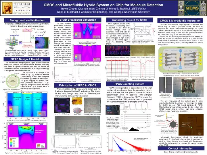
CMOS and Microfluidic Hybrid System on Chip for Molecule Detection Bowei Zhang, Qiuchen Yuan, Zhenyu Li, Mona E. Zaghloul , IEEE Fellow Dept. of Electrical & Computer Engineering, The George Washington University. SPAD Breakdown Simulation. Quenching Circuit for SPAD.

E N D
CMOS and Microfluidic Hybrid System on Chip for Molecule Detection Bowei Zhang, Qiuchen Yuan, Zhenyu Li, Mona E. Zaghloul, IEEE Fellow Dept. of Electrical & Computer Engineering, The George Washington University SPAD Breakdown Simulation Quenching Circuit for SPAD Background and Motivation CMOS & Microfluidic Integration Scientific and Medical Fluorescence Image System needs to detect very weak photon signal For p+/n- junction photodiode, when the p+ doping density fixed, the lower the n- doping density, the higher the breakdown voltage. When the doping density at the perimeter area of the photodiode is low enough, the junction would breakdown at the center area first. Therefore, by control the gap between two n-wells, a low doping n- guard ring can be created to prevent the perimeter breakdown. Fig. 2&3 show the simulation results. When a photon arrives, SPAD breakdown, a quenching circuit is required to pull down the reverse voltage after an avalanche event, and after the recombination of the electron in the junction, the quenching circuit will apply a high reverse voltage on the SPAD again to ready for detecting another photon. Traditional fluorescence image system is complex and relative big. To build a portable system, we want to integrated the CMOS & Microfluidic technology. The hybrid CMOS & Microfluidic system is much smaller compare with traditional optics setup. It also have the potential to reach the similar sensitivity as the traditional setup. we use the material call polydimethylsiloxane (PDMS) to make the Microfluidic channels. PDMS is a soft polymer widely used in microfluidic and micro-optics due to its low cost, easy fabrication process, bio-compatibility and optical transparency. Lost Energy Time Delay Wavelength Lifetime “Delay control signal” controls the rising delay of a slow rise inverter, which could adjust the output pulse width Fig.2(a) Simulated current density with proper n-wells gap(1.8um) Lifetime Fluorescence excitation process Traditional image system use 3 filters at each pixel to identify different wavelength, which waste 2/3 of the photon signal. lifetime image system doesn’t need filter. Each pixel use lifetime to distinguish signals. Sensitivity can be improved about 3 times. 10μm Layout design of Dynamic Quenching Circuit Fabricated CMOS Dynamic Quenching Circuit SPAD Design & Modeling For fluorescence image system, signal photon avalanche diode(SPAD) can be used as the photon detector. It not only can detect the photon numbers, but also can detect the fluorescence lifetime. We used the CMOS 0.5μm technology to design and fabricated the SPAD. Fig.2(b) Simulated current density, when n-wells gap too small, breakdown happened at perimeter The top view of our design is as shown in Fig.1 (a). A center n-well and a surrounding n-well were designed with certain gap between each other . The guard ring gap can protect SPAD from perimeter breakdown. A p+ doping is designed to cover the center n-well to form a p+n- juction, which is the area to detect photons. Design diagram of hybrid CMOS & Microfuidic System. Microfluidic channels are used for electrical interconnection and sample delivery Output from Dynamic Quenching Circuit Each pulse indicate one photon event Each pulse has around 45ns pulse width Fig.3(b) Simulated quantum efficiency Fig.3(a) Simulated I-V character of SPAD FPGA Counting System Fabrication of SPAD in CMOS FGPA counting system is design to count the total number of signal pulse from the quenching circuit, which indicates the total photon number in certain accumulation time. In addition, Time-to-Digital Converter (TDC) is designed on FGPA to record the photon arrive time. Which can be used to generated the fluorescence lifetime after signal processing. After simulation, SPAD, Quenching circuit and I/O Pads are designed in CMOS technology. The layout of the chip design was sent to semiconductor manufacturing company for fabrication. Fig.1(a) SPAD design top view 100μm 80um microfluidic channel delivering low melting point solder 200μm Preliminary CMOS & Microfluidic Hybrid System The key innovations of this method are: 1. using microfluidic channel to delivery low melting point solder for CMOS die and PCB board bonding. 2. PDMS Microfluidic channela put test sample directly contact with CMOS sensor chip to achieve high signal collection efficiency, thus improve the sensitivity. CMOS Foundry 500μm Layout of our SPADs design Silicon Wafer Fabricated chip of SPAD design Altera Cyclone II FGPA board used for design counting system. The figure on the right shows the basic function of Time correlated Single Photon Counting (TCSPC), which embedded in FPGA Fig.1(b) Device doping profile model based on CMOS 0.5 μm Technology . Coated micro-beads that can catch target molecule and generate fluorescence signal. 25μm 20μm 9 SPAD Designs with different Guard Ring Gap length Microbead fluorescence signal in preliminary experiment. A microfluidic channel trap is designed to catch a 10um diameter micro-bead with fluorescence signal. Our further work is to integrate this trap right on top of the SPAD Two samples with different fluorescence lifetime Contact Information Measured I-V character of one of the fabricated SPAD with proper guard ring gap length(1.8um) Measured I-V character of one of the fabricated SPAD with wrong Gap length Bowe Zhang, email: bowei@gwmail.gwu.edu Fig.1(c) Device electric field profile. High electric field area easier to breakdown.