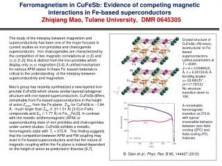
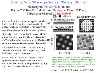
Download
1 / 1
10 likes | 235 Vues
Pulsed Laser Plasmonic Welding of Ag Nanowires for Transparent Conducting Layers Nai Phuan Ong , Princeton University, DMR 0819860 Princeton Center for Complex Materials (PCCM).

E N D
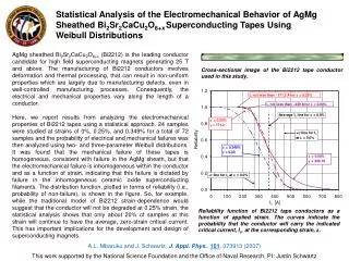
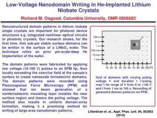
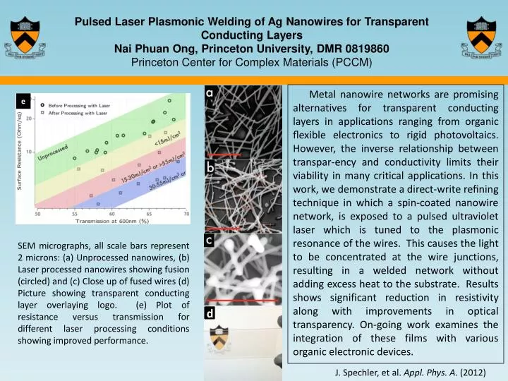
Pulsed Laser Plasmonic Welding of Ag Nanowires for Transparent Conducting Layers NaiPhuanOng, Princeton University, DMR 0819860Princeton Center for Complex Materials (PCCM) Metal nanowire networks are promising alternatives for transparent conducting layers in applications ranging from organic flexible electronics to rigid photovoltaics. However, the inverse relationship between transpar-ency and conductivity limits their viability in many critical applications. In this work, we demonstrate a direct-write refining technique in which a spin-coated nanowire network, is exposed to a pulsed ultraviolet laser which is tuned to the plasmonic resonance of the wires. This causes the light to be concentrated at the wire junctions, resulting in a welded network without adding excess heat to the substrate. Results shows significant reduction in resistivity along with improvements in optical transparency. On-going work examines the integration of these films with various organic electronic devices. e d SEM micrographs, all scale bars represent 2 microns: (a) Unprocessed nanowires, (b) Laser processed nanowires showing fusion (circled) and (c) Close up of fused wires (d) Picture showing transparent conducting layer overlaying logo. (e) Plot of resistance versus transmission for different laser processing conditions showing improved performance. J. Spechler, et al. Appl. Phys. A. (2012)


![[1] J. Zhang et al. , Appl. Phys. Lett . 88 , 123112 (2006).](https://cdn2.slideserve.com/3783086/slide1-dt.jpg)