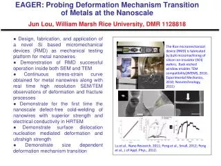
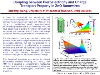
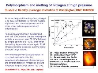
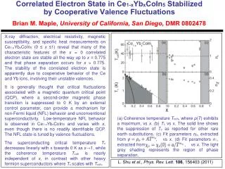
Download
1 / 5
50 likes | 128 Vues
Scanning Probe Microscopy Studies of Polycrystalline and Nanocrystalline Semiconductors Reuben T. Collins, Colorado School of Mines, and Thomas F. Kuech, University of Wisconsin, DMR-0103945.

E N D
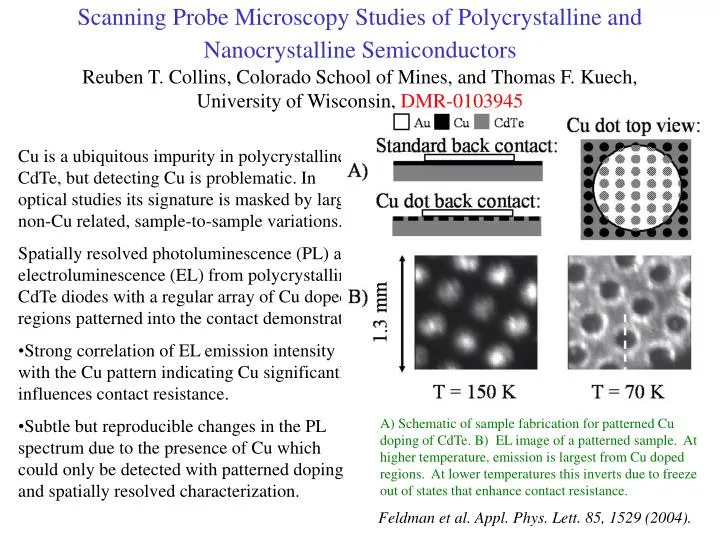
Scanning Probe Microscopy Studies of Polycrystalline and Nanocrystalline SemiconductorsReuben T. Collins, Colorado School of Mines, and Thomas F. Kuech, University of Wisconsin, DMR-0103945 • Cu is a ubiquitous impurity in polycrystalline CdTe, but detecting Cu is problematic. In optical studies its signature is masked by large non-Cu related, sample-to-sample variations. • Spatially resolved photoluminescence (PL) and electroluminescence (EL) from polycrystalline CdTe diodes with a regular array of Cu doped regions patterned into the contact demonstrate: • Strong correlation of EL emission intensity with the Cu pattern indicating Cu significantly influences contact resistance. • Subtle but reproducible changes in the PL spectrum due to the presence of Cu which could only be detected with patterned doping and spatially resolved characterization. A) Schematic of sample fabrication for patterned Cu doping of CdTe. B) EL image of a patterned sample. At higher temperature, emission is largest from Cu doped regions. At lower temperatures this inverts due to freeze out of states that enhance contact resistance. Feldman et al. Appl. Phys. Lett. 85, 1529 (2004).
Cu is a particularly important impurity in CdTe. It is a common contaminant in CdTe films, and, in addition, is commonly included during contact formation procedures where it functions as a p-type dopant initially lowering contact resistance. Polycrystalline CdTe device stability, however, has been correlated with rapid Cu diffusion from the contact into the CdTe active region. We have used spatially resolved electroluminescence (EL) in combination with photoluminescence (PL) to study Cu impurities in CdTe. Polycrystalline CdS/CdTe heterojunction diodes were prepared in the manner typically followed in making solar cell devices. During preparation, the back surface of the CdTe was non-uniformly doped (in advance of contact formation) with Cu evaporated through a shadow mask composed of 150μm diameter circles. EL emission from the completed device was then spatially imaged as a function of temperature using our high sensitivity CCD detector. EL emission correlated well with the location of the Cu dots as shown by the images in the figure. From room temperature down to approximately 100 K, EL intensity was up to an order of magnitude greater on the Cu dots. This result is consistent with the idea that the presence of Cu reduces back contact resistance. Below 100 K, the EL pattern inverted, with the intensity from non-Cu regions up to an order of magnitude more than from Cu dot regions. This inversion is attributed to freeze out of Cu related defect levels contributing to conduction. The ability to definitively identify the Cu doped regions through EL measurements allows us to perform spatially resolved PL measurements on exactly the same sample region and correlate PL spectra with the presence or absence of Cu. The PL showed no correlation with the Cu pattern when integrated over all energies. However, PL originating from deep states near 1.35eV was slightly more intense in Cu-doped regions. This spectral range has been associated with Cu on a Cd site in the literature. In contrast, the intensity of PL from shallower states near 1.5 eV which are commonly associated with Cd vacancies was slighlty greater in non-Cu-doped regions. The small differences between PL spectra from Cu doped and undoped regions provide an optical signature of the presence of Cu which was discernable only with the patterned doping and spatially resolved characterization used here. Prior studies of Cu doping have used two different samples, one doped and one without doping. Sample to sample variations, however, in luminescence properties were typically much larger than the small Cu related effects observed here making it impossible to draw conclusions from these earlier studies. The results of this work were published in “Effects of Cu in CdS/CdTe solar cells studied with patterned doping and spatially resolved luminescence,” S. D. Feldman, R. T. Collins, V. Kaydanov, and T. R. Ohno, Appl. Phys. Lett. 85, 1529 (2004).
Scanning Probe Microscopy Studies of Polycrystalline and Nanocrystalline SemiconductorsReuben T. Collins, Colorado School of Mines, and Thomas F. Kuech, University of Wisconsin, DMR-0103945 • Education/Outreach: A central theme has been involvement of undergraduate students in research early in their career. • Four undergraduate REU students have become active and valued members of the research team. • Students participate in group meetings, give conference presentations, write reports and publish papers. • During 2004 Regina Caputo was co-author on an Applied Physics Letter. Joshua Dorr completed a research project that is being prepared for publication with Josh as first author. Both presented posters at the annual Rocky Mountain Chapter of the AVS and participated in outreach to the local community. Joshua Dorr and Regina Caputo at the annual meeting of the Rocky Mountain chapter of the AVS and with Denver 9-News anchor Ward Lucas demonstrating a home made solar oven for a news spot on “How hot is it?”
Education: This project has directly involved two graduate students at CSM, Kristin Galbally and John Yarbrough, and one at the Univ. of Wisconsin, Anish Khandekar. Four undergraduates, Matt Treaster, Nate Hamm, Regina Caputo, and Josh Dorr have also participated in meaningful research projects through summer REU support. One of the graduate students (K. Galbally, MS in Materials Science, 2002, now at Directed Energy Solutions) and two of the undergraduates (N. Hamm, BS in Eng. Physics, 2003, now a graduate student in Engineering at CSM, and M. Treaster, BS in Eng. Physics, 2004) have completed their degrees. Two post docs, Cecile Veauvy and Joe Beach, and three additional grad students, Scott Feldman, Ian Schick, and Cary Allen, while not directly supported by the project, have profited from involvement in it. Undergraduate participation in the project has been an important human resource emphasis, and in many ways one of the most pleasant aspects of the project. Undergraduates are integrated into the group as regular members. All of the undergrads maintained their involvement from the first summer as REU students until the present time (or they graduated) working with the team during the school year and subsequent summers. They have desks in the graduate student office. In addition to developing research expertise, undergraduate communications skills are honed. The students attend group meetings and give regular presentations on their work. They are critiqued and actively participate in critiquing the graduate students’ (and the advisor’s) presentations. They also present and publish their research. In the last year Regina Caputo’s PL research led to co-authorship of a publication (“Formation of regular arrays of submicron GaAs dots on silicon,” J. D. Beach , A. A. Khandekar , C. K. Inoki , C. Veauvy , R. Caputo , R.T. Collins , T. F. Kuech , T. S. Kuan , and R. E. Hollingsworth, Appl. Phys. Lett.84, 5323 (2004)). Joshua Dorr has developed a new surface treatment for stamps used in microcontact lithography that allows salts dissolved only in water or water and solvent to be patterned on Si. Josh is preparing this work for publication. Regina and Josh both gave posters at the 2004 annual meeting of the Rocky Mountain chapter of the AVS as shown in the photos. It was their first experience at giving a true technical presentation.
Outreach: Public visits to the Colorado School of Mines campus are frequent (visitation days for prospective students and their parents, tours of the minority engineering program, etc.) and the PIs lab and projects are often a stop on these tours. Students and advisor use these opportunities to tell the public, often in layman’s terms, about on-going projects and the value of materials science. An interesting example this summer involved a very hot day when a local television news program called the school for help on a spot discussing the heat. Regina Caputo and Josh Dorr took a day off from their research to help physics department professor, Tom Furtak, assemble a solar oven from common household items. They then made “smores” on camera. The photo shows Josh, Regina, Tom, Barbara Johnson (the department administrative assistant) and 9-news anchor Ward Lucas. The spot appeared on the 6:00pm news.

![[1] J. Zhang et al. , Appl. Phys. Lett . 88 , 123112 (2006).](https://cdn2.slideserve.com/3783086/slide1-dt.jpg)