Download
1 / 24
250 likes | 612 Vues
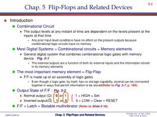
Ch.8 Flip-Flops and Related Devices. Latch Edge-Triggered and Master-Slave Flip-Flops Flip-Flop Operating Characteristics Flip-Flop Applications One-Shots and the 555 Timer Troubleshooting Programmable Logic: Registered Operation Latches and Flip-Flops Using VHDL. Y=f(X). X. f. n. m.

E N D
Ch.8 Flip-Flops and Related Devices Latch Edge-Triggered and Master-Slave Flip-Flops Flip-Flop Operating Characteristics Flip-Flop Applications One-Shots and the 555 Timer Troubleshooting Programmable Logic: Registered Operation Latches and Flip-Flops Using VHDL
Y=f(X) X f n m Introduction Digital Logic (1) Combinational Logic Circuit, (2) Sequential Logic Circuit Combinational Logic Circuit X: the finite set of input symbols Y: the finite set of output symbols f: a Boolean function for the output
Sequential Logic Circuit Latches, Flip-flops RAM, etc.
f g X Y=f(X,S) n m K S Storage Device S+=g(X,S) Status Finite State Machine X : the finite set of input symbols Y : the finite set of output symbols S : the finite set of status symbols, S 2K f : a Boolean functions(logic diagram) for output Y g : a Boolean functions for next state S+
Latches • The S-R (Set-Reset) Latch • A type of bistable multivibrator • Store one bit (걸쇄, 빗장) Figure 8-1 Two versions of SET-RESET (S-R) latches. Open file F08-01 and verify the operation of both latches.
QQ’=1 Normally HIGH input
Application Example : Latches • The Latch as a Contact-Bounce Eliminator S’: 1 1 1 1 • • • 1 0 1 0 0 • • • R’: 0 1 0 1 • • • 1 1 1 1 1 • • • No change
The Gated S-R Latch • Requires an enable input(EN) (G is also used to designate an enable input) 1 0 1 Figure 8-7 A gated S-R latch.
Edge-Triggered Flip-Flops • Edge-triggered flip-flop changes state either at the positive edge(or rising edge) or at the negative edge(falling edge) of clock pulse and is sensitive to its inputs only at this transition of clock + T-flip-flop Figure 8-11 Edge-triggered flip-flop logic symbols (top: positive edge-triggered; bottom: negative edge-triggered).
The Edge-Triggered D Flip-flop Figure 8-18 A positive edge-triggered D flip-flop formed with an S-R flip-flop and an inverter/ truth table
The Edge-Triggered J-K Flip-flop Figure 8-20 A simplified logic diagram for a positive edge-triggered J-K flip-flop. toggle Figure 8-21 Transitions illustrating the toggle operation when J=1 and K=1.
State Equation of J-K Flip-flop State Equation Q(t+1) = JQ(t)’ + K’Q(t)
The Edge-Triggered T Flip-flop T Clk T Q
Master-Slave Flip-Flops • The pulse-Triggered Master-Slave J-K Flip-flop slave master Figure 8-28 Basic logic diagram for a master-slave J-K flip-flop.
Input J K Clk Output Q Q’ Comments 0 0 Q Q’ No change 0 1 0 1 Reset 1 0 1 0 Set 1 1 Q’ Q Toggle Ex 8-9) For a active LOW clock master-slave J-K flip-flop, determine the Q output waveform