Download
1 / 13
150 likes | 672 Vues
Choice of PLL : type II 3rd order . Power consumption < 1mWFrequency of operation:Reference from power link: 1MHz Data carrier: 32MHz We operate the VCO at twice the data carrier frequency (64Mhz) to get good 50% duty cycle after dividing by 2.Parts: PFD, ChargePump 2nd order passive filter voltage controlled 3-stage ring-oscillator 1/64 frequency divider.

E N D
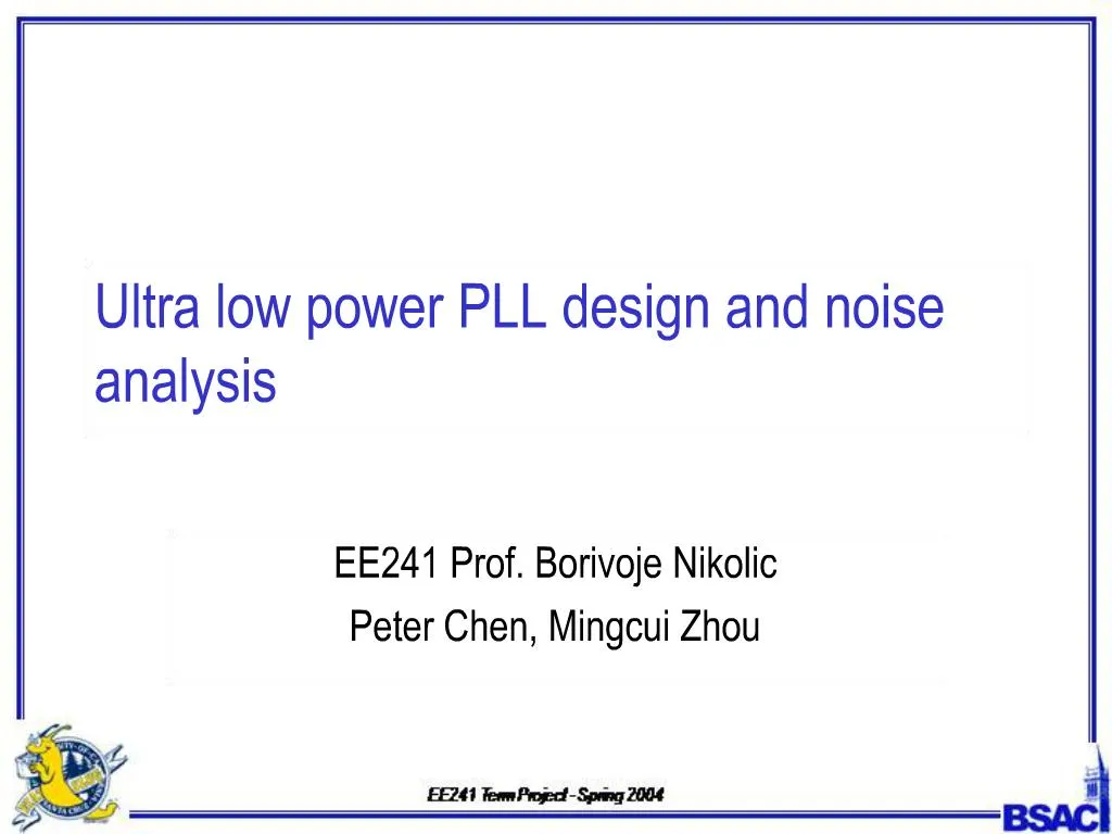
1. Ultra low power PLL design and noise analysis EE241 Prof. Borivoje Nikolic
Peter Chen, Mingcui Zhou
2. Choice of PLL : type II 3rd order Power consumption < 1mW
Frequency of operation:
Reference from power link: 1MHz
Data carrier: 32MHz
We operate the VCO at twice the data carrier frequency (64Mhz) to get good 50% duty cycle after dividing by 2.
Parts:
+ PFD, ChargePump
+ 2nd order passive filter
+ voltage controlled 3-stage ring-oscillator
+ 1/64 frequency divider
3. System block diagram
4. Tracking time Using Matlab determine the optimum loop filter parameter for enough phase margin and settling time.
Loop filter choice:
Cp=2uF, R=10k
C2=42pF
damping= 0.66
Settling =60us
~60 times reference frequency.
Cp C2 is shown in the previous slides, the function of C2 is to make it more stablilized, and usually at least 10 times smaller than CpCp C2 is shown in the previous slides, the function of C2 is to make it more stablilized, and usually at least 10 times smaller than Cp
5. Block design: VCO 3 stages of oscillator is mainly of power concern:
Two ways to decrease the oscillation frequency: 1st, more stages� more power, 2nd, longer channel length, increase the intrinsic delay ***asymetry in the system cause uneven rise full time, and cuz more phase noise,*** the reason to increase the frequency to 64MHz then divided by to for output is to tune the duty cycle to 50%.
Add pass gate to equalize lag
3 stages of oscillator is mainly of power concern:
Two ways to decrease the oscillation frequency: 1st, more stages� more power, 2nd, longer channel length, increase the intrinsic delay ***asymetry in the system cause uneven rise full time, and cuz more phase noise,*** the reason to increase the frequency to 64MHz then divided by to for output is to tune the duty cycle to 50%.
Add pass gate to equalize lag
6. Frequency Divider
7. Phase Frequency Detector and Charge Pump
8. Simulation Result We used both spectre and hspice to do the simulation:
Hspice for calculating the jitter and spectre for pss noise analysisWe used both spectre and hspice to do the simulation:
Hspice for calculating the jitter and spectre for pss noise analysis
9. Power dissipation VCO power=225.7uW
@ 64MHz supply=1.8v
PFD and charge pump power=53.7uW
the main power drain is bias branch for charge pump
Divider power=4.176uW @ 64MHz
Total power=280.3uW
When VCO operate at fmax=140MHz, the total power of the PLL is still under 1mW.
Specs achieved.
blue: VCO
red: divider N=64
Green: charge pump.
10. Noise in PLL: low pass, high pass Noise from each source can be modeling using transfer function from it�s generation place to the output,
Sleq = pfd & CP
Noise from each source can be modeling using transfer function from it�s generation place to the output,
Sleq = pfd & CP
11. Noise of PLL: synchronous/Accumulating jitter Explain the thing in the phase domain���as we discussed, the VCO cloose looop gain is shown as high passExplain the thing in the phase domain���as we discussed, the VCO cloose looop gain is shown as high pass
12. Noise generation in PFD/CP Noise mechanism in PFD
Current mismatch in charge pump pull down, pull up network
Leakage current
Reset delay
Up/Down Signal arriving time difference.
Decreasing the transistor size and bias current lower power dissipation at the expense of mismatch Point to the red line in the picture, there�s leakage shown, red is the output of dividr, blue is the refernce, when blue lead read 1, Vctrl should increase due to Up signal =1, however, when both signal is high, there�s DC current flow through the Charge pump, and mismatch in this case cuz charing or discharging of the capacitor. it takes a while for the reset to set both UP and Down signal low, and it can be shown that the Point to the red line in the picture, there�s leakage shown, red is the output of dividr, blue is the refernce, when blue lead read 1, Vctrl should increase due to Up signal =1, however, when both signal is high, there�s DC current flow through the Charge pump, and mismatch in this case cuz charing or discharging of the capacitor. it takes a while for the reset to set both UP and Down signal low, and it can be shown that the
13. VCO noise The main noise contributor in a PLL
i) Transistor thermal noise
ii) Supply/substrate noise:
measured supply gain to output frequency:
Ks=0.3MHz/v
57dB difference compared to Kv
Using Spectre calculating steady state phase noise of oscillator
(Without supply/substrate noise)
12.8dBc @ 2.5MHz
1/f roll-off For Kv=200MHz/v, it�s 56dBFor Kv=200MHz/v, it�s 56dB
14. Conclusions Don�t even think about all-digital PLL (ADPLL) if you want very low-power operation
A novel low-power and low noise VCO design would be very attractive (e.g. MEMS?)