Download
1 / 27
270 likes | 275 Vues
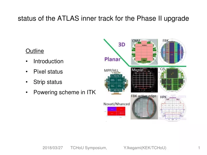
Outline Introduction Pixel status Strip status Powering scheme in ITK. status of the ATLAS inner track for the Phase II upgrade. Present ATLAS inner tracker. (4 layers). (4 layers). (9 layers). Pixel + SCT (strip) + TRT (chamber) x10 higher luminosity phase II upgrade (HL-LHC)

E N D
Outline • Introduction • Pixel status • Strip status • Powering scheme in ITK status of the ATLAS inner track for the Phase II upgrade 2018/03/27 TCHoU Symposium, Y.Ikegami(KEK/TCHoU)
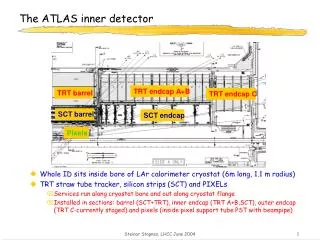
Present ATLAS inner tracker (4 layers) (4 layers) (9 layers) Pixel + SCT (strip) + TRT (chamber) x10 higher luminosity phase II upgrade (HL-LHC) ⇒ All silicon semiconductor inner tracker (ITK) 2018/03/27 TCHoU Symposium, Y.Ikegami(KEK/TCHoU)
ATLAS detector to design for • Instantaneous lum.: 7x1034 cm-2s-1 • Integrated lum.: 6000 fb-1 (including safety factor 2 in dose rate) • Pileup: 200 events/crossing • PIXELs (HL-LHC) • Inner: r=3.7 cm ~2.2x10¹⁶ • Medium: r = 7.5 cm, ~6x10¹⁵ • Med/Out: r=15.5 cm ~2x10¹⁵ • Outer: r = 31 cm (?) ~1x10¹⁵ • STRIPs (HL-LHC) • Replacing Strip and TRT • r = 30 cm, e.g. • Fluence ~1x10¹⁵ occupancy⇒pixel size :50 x 400 →50 x 50 or 25 x 100 (μm) strip length: 120 → 24 (mm) Radiation damage⇒p-bluk sensor Impact to ITK for phase II upgrade 2018/03/27 TCHoU Symposium, Y.Ikegami(KEK/TCHoU)
LHC schedule machine shutdown machine shutdown mass production start ~5 years production Installation start start HL-LHC 2018/03/27 TCHoU Symposium, Y.Ikegami(KEK/TCHoU)
ITK Layer 7 strip Layer 6 strip Layer 5 strip Layer 5 strip Layer 4 CMOS Layer 3 planar Layer 2 planar Layer 1 planar Layer 0 3D 2018/03/27 TCHoU Symposium, Y.Ikegami(KEK/TCHoU)
FEI3 present pixel layer 1,2,3 (250nm) Pixel size 50x400 (μm) • FEI4 present pixel layer 0 (130nm) upgrade R&D target pixel size 50x250 (μm) • ENC ~100e for 50x50 (μm) pixel • FE65p2 analog part test version (65nm) limited digital function and small chip size target pixel size 50x50 (μm) ENC ~40e for 50x50 (μm) pixel: twice as much improvement. • RD53A semifinal version (65nm) • Detailed inspection is ongoing • Probed chips will be delivered soon. • RD53B final version has been designed. Pixel FE ASIC 2018/03/27 TCHoU Symposium, Y.Ikegami(KEK/TCHoU)
Detector input capacitance 2018/03/27 TCHoU Symposium, Y.Ikegami(KEK/TCHoU)
ENC 50x50 um FE No bias rail Outer layer: Planar Pixel sensor Sensor w/o bias rail We cannot do the initial tests w/o bias rail structure. HPK will not deliver no inspected sensors. w/ bias rail Sensor w/o bias rail Initial IV test can be done w/o FE. As the pixel size became smaller, the difference became larger. 2018/03/27 TCHoU Symposium, Y.Ikegami(KEK/TCHoU)
Bias structure optimization • We need optimization for bias structure. • Lower inter-pixel capacitance • Higher resistivity of bias resister • We have been investigating sensor variations in new 6th mask. 2018/03/27 TCHoU Symposium, Y.Ikegami(KEK/TCHoU)
Innermost layer 0: 3D pixel • Pillars in 3D pixel are implemented at 50 (μm) intervals. • We obtain sufficient signals at low voltage sensor operation and expect high radiation tolerance. • Major Sensor vender: • CNM (Barcelona) • FBK (Trento, Italy) • These look like National Institute of Advanced Industrial Science and Technology (AIST). • There is a limit to mass production capacity. Full depilation voltage [V] 2018/03/27 TCHoU Symposium, Y.Ikegami(KEK/TCHoU)
Cost effective ~1/3 • ⇒ no bump bonding • Radiation tolerance < 5x10¹⁴ neq/cm2 • ⇒ layer 4 • Survived full size (>10mmx10mm) 3 prototypes: Outermost layer 4: CMOS monolithic pixel LFoundry (150nm) AMS (180nm) TowerJazz (180nm) Rad. Hard Large Cdet large fill-factor small fill-factor 2018/03/27 TCHoU Symposium, Y.Ikegami(KEK/TCHoU)
The development of the analog part is almost completed. The development of the interface part is urgent. Outermost layer 4: CMOS pixel to do ~500um: interface part 2018/03/27 TCHoU Symposium, Y.Ikegami(KEK/TCHoU)
UBM +bump forming Pixel module (FEI4) UBM Under Bump Metallization: Clean up surface of pad Flip chip bump bonding Pixel module Quad module: Sensor x1 + FE x4 Sensor size: 40mm x 40mm flex PCB After bending flex PCB 2018/03/27 TCHoU Symposium, Y.Ikegami(KEK/TCHoU)
Strip sensor Long term instability was reported. J. Suzuki was found humidity dependence. New passivation scheme was proposed and resolved. Market survey is ongoing. HPK will be ready for mass production. 2018/03/27 TCHoU Symposium, Y.Ikegami(KEK/TCHoU)
After the first ABC ASICs (named ABC130) were designed and fabricated on the IBM 130nm technology, the ATLAS trigger rate requirement was increased to 1 MHz. • The ABC130/HCC readout architecture could not support this 1 MHz rate and, therefore, a design change was required. • First Star Chips and preliminary testing in the summer, 10 wafers in the fall and push for star module test beam in October Strip FE ASIC 2018/03/27 TCHoU Symposium, Y.Ikegami(KEK/TCHoU)
CMOS power consumption ∝ CV2 • Low power consumption ⇒ low V, C • Module: V~1V, I~1A ~ 1Ω • RCu cable : L~100m, S~1mm2~10Ω • In order to match gaps, ATLAS will introduce: • DC/DC converter for strip • Serial power scheme for pixel Powering scheme for ITK upgrade 2018/03/27 TCHoU Symposium, Y.Ikegami(KEK/TCHoU)
High magnetic field ⇒ Air-core coil • ⇒ high frequency operation: 1~3MHz • ⇒ tight noise shield • “FEATS2” was developed by CERN • input voltage range 5 to 12V • 4A load capability • Radiation tolerant: TID up to >200Mrad(Si) and 5x10¹⁴ neq/cm2 Powering scheme: DC/DC converter and strip module DC/DC converter ABC130 Strip module 2018/03/27 TCHoU Symposium, Y.Ikegami(KEK/TCHoU)
Idea is simple: Powering scheme: Serial powering Serial individual 2018/03/27 TCHoU Symposium, Y.Ikegami(KEK/TCHoU)
Shunt regulator constant current source Realistic serial powering system FE PSPP (Pixel Serial Power Protection) bleeder current ⇒I operation > I maximum module bypass circuit ⇒ MOS Tr. 2018/03/27 TCHoU Symposium, Y.Ikegami(KEK/TCHoU)
Flip chip module Module flex tail part PSPP chip Serial powering at ATLAS PIXEL and demonstrator • 7 quad pixel modules will be installed for system tests. • first 4 modules were made by Japan cluster. • This demonstrator has no bus tape. 2018/03/27 TCHoU Symposium, Y.Ikegami(KEK/TCHoU)
2018/03/27 TCHoU Symposium, Y.Ikegami(KEK/TCHoU)
A status of the ATLAS inner track for the Phase II upgrade was presented. • There are still many works to do before mass production. Up to now, there is no show stopper… • Pixel sensor : final tuning for bias rail structure • Pixel FE : semifinal ASIC tests on going • Strip sensor : ready to mass production • Strip FE : “star” ASIC in this summer. Summary 2018/03/27 TCHoU Symposium, Y.Ikegami(KEK/TCHoU)
backup 2018/03/27 TCHoU Symposium, Y.Ikegami(KEK/TCHoU)
ATLAS detector 2018/03/27 TCHoU Symposium, Y.Ikegami(KEK/TCHoU)
Inner detector layer structure 2018/03/27 TCHoU Symposium, Y.Ikegami(KEK/TCHoU)
現行のNバルクセンサー N 全空乏化させて十分な信号量を得る シリコン半導体検出器の放射線損傷 照射によりN→P 全空乏化させないと電極分離しない 1014 /cm2(LHC当初計画)を越えると全空乏化電圧は500Vに達し、システムの耐圧を越える 衝突で発生する粒子により、P型不純物が生成される N型バルク:P型に反転した後に全空乏化電圧が上昇 放射線耐性をさらに上げるには、 P型バルクセンサー 型反転しない PN接合側の電極は部分空乏化でも分離 耐圧を越えたら、電圧を下げて運転(信号量は減る)
+ + + + + + + + + + • - - - - - - - n+ n+ 電極間の分離 酸化膜SiO2に正電荷が蓄積し、Pバルク部表面に引き寄せられた 電子のために、ストリップ間が電気的に繋がってしまう。 P型半導体によるシリコン検出器の課題 SiO2 n+ n+ n+ n+ n+ n+ p+ p+ P-spray P-stop P-spary, P-stop, geometry, implant condensation, … 1cm x 1cm のbaby sensor用いて、照射試験を行い性能を比較