Download

1 / 14
140 likes | 238 Vues
An Analog Wavelet Transform CMOS Imager Chip. Adeel Abbas, Saurav Panda, Vikram Shirgur Graduate Advisor: Shantanu Chakrabartty 520.490 Analog and Digital VLSI Systems. Motivations. Hardware Implementation of Image Compression Small size

E N D
An Analog Wavelet Transform CMOS Imager Chip Adeel Abbas, Saurav Panda, Vikram Shirgur Graduate Advisor: Shantanu Chakrabartty 520.490 Analog and Digital VLSI Systems
Motivations • Hardware Implementation of Image Compression • Small size • Reconfigurable to compute user-defined functions (e.g. Walsh Transform, Hadamard Transform) • Edge detection, pattern matching
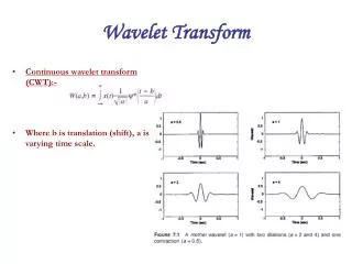
Wavelet Transform Theory • Multi-resolution feature extraction • Many basis functions available, Haar Wavelet implemented • Haar transform is a combination of summing and difference operations
Hardware Implementation • Haar Transform can be realized as a Matrix Vector Multiplication problem • W (i,j) = ( ΣA(i)×P(i,j) ) × B(j) • Multiply with either +1, 0 or -1 • Inputs are presented in bit-serial fashion
System Architecture • 16 x 24 pixel array • 2 CDS stages for inner and outer products • Product coefficients input through shift registers
The APS Cell • Charge mode implementation • Product Coefficient provided in two phases • Output of all cells is dumped to a common line • Charge is either dumped or extracted from output line
The APS Cell (Layout) • Uses photodiode type design • Susceptible to mismatches in transistor sizing • Fill Factor: 60 % • Dimensions: 89λ x 89λ
CDS Circuit • Cascoded inverter used for high gain • Phase of B(i) determines whether we connect output capacitor to CDS or Vref • CDS stage 1 adds charge across columns, Stage 2 adds output of CDS circuits in stage 1
Simulation of APS And Inner Product • Operating Frequency of 11KHz • Photocurrent of 60pA • Sequencing of 1st and 2nd stage clocks is very important • Here we are multiplying by -1
Simulation Results for Outer Product (4×4) • Here again we are multiplying by -1 • Output valid during Hold phase of stage 2 • Voltage range of 1.76V to 4.23V, with reference at nearly 3 V
Future work • Parallel readout (currently can be used as a random-access imager) • Extend for a 3 x 3 pad-frame. Would allow a resolution of around 72x72 • More test pins. Currently the chip utilizes 29 pins