Download
1 / 12
130 likes | 272 Vues
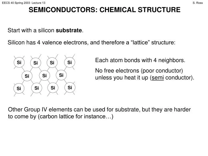
Si. Si. Si. Si. Si. Si. Si. Si. Si. Si. Si. SEMICONDUCTORS: CHEMICAL STRUCTURE. Start with a silicon substrate . Silicon has 4 valence electrons, and therefore a “lattice” structure:. Each atom bonds with 4 neighbors.

E N D
Si Si Si Si Si Si Si Si Si Si Si SEMICONDUCTORS: CHEMICAL STRUCTURE Start with a silicon substrate. Silicon has 4 valence electrons, and therefore a “lattice” structure: Each atom bonds with 4 neighbors. No free electrons (poor conductor) unless you heat it up (semi conductor). Other Group IV elements can be used for substrate, but they are harder to come by (carbon lattice for instance…)
Si Si Si Si Si Si Si Si Si As Si Si Ga Si Si Si Si Si Si Si Si Si e DOPING Make silicon a better conductor by adding Group III or Group V elements: process called doping Add Group III elements like gallium or indium to get p-type material Note that the Ga atom has only 3 valence electrons with which to bond; missing bond is called a hole hole Add Group V elements like arsenic or phosphorus to get n-type material Note that the As atom has 5 valence electrons; it has an unbonded electron Materials are electrically neutral! Equal number of protons and electrons!
e e e h h h e e e h h h p-type extra holes n-type extra e- aluminum e e e h h h P-N JUNCTION: THE BASIS FOR ELECTRONICS Put p-type and n-type material together: Essential Property: Make current flow (or not flow) by applying electric field (voltage) to metal ends. - + This is a diode. “Voltage Controlled Switch”
h h - e e e h h h + e e e e h h h h h - e + e e e e e h h h h h - + e e PHYSICS OF P-N JUNCTIONCASE: Open Circuit Free electrons from n-type are chemically attracted to holes in p-type. Free electrons move across junction to fill holes: process called diffusion Unbalanced protons are left in n-type, unbalanced electrons now in p-type. a n-type p-type n-type p-type Area near p-n junction now has no charge carriers (free electrons or holes): called depletion region depletion region V The charged atoms in the depletion region create an electric field, and thus a difference in electric potential. dist from junction When the potential drop becomes steep, the free electrons no longer cross: drift takes over
h h - + e e h h - + e e h h - + e e PHYSICS OF P-N JUNCTIONCASE: Short Circuit Is there a current when I short a diode? Is KVL violated? NO. n-type p-type At metal-semiconductor junction, potential changes to balance device. Electrons in metal can redistribute easily to do this. metal contact V metal contact dist from junction
p-type n-type – – e + + – – e + + h – – e + + h h depletion region (no free e, h) – + VS > 0 metal contact V VS dist from junction metal contact PHYSICS OF P-N JUNCTIONCASE 2: Reverse Bias A diode is in reverse bias mode when the + (p-type) terminal is at a (moderately) lower potential than the – (n-type) terminal. Electrons bunch up by positive metal contact, but few cross through wire because of potential drop between contacts. A tiny “leakage current” flows due to these few stray electrons, but basically zero current flow.
h h h – + metal contact V VS dist from junction PHYSICS OF P-N JUNCTIONCASE: Reverse Breakdown p-type n-type When the diode + terminal is at a much lower potential than the - terminal, reverse breakdown occurs. Reverse breakdown begins when the potential rise across the junction becomes so great that electrons from the p-type material travel across the rise. The difference in potential has to be great enough to overcome the chemical bonds in the p-type lattice. – – e + + e – – e + + e – – e + + depletion region (no free e, h) VS > VZK metal contact Voltage necessary for breakdown: VZK “Zener knee”
- + PHYSICS OF P-N JUNCTIONCASE: Reverse Breakdown • There are diodes called Zener diodes that are designed to operate in reverse breakdown. • The voltage across the diode in the reverse breakdown mode is about constant, as once the voltage gets past VZK, the depletion layer does not really increase—the current increases dramatically (also known as avalanche current). • As the reverse voltage is increased, there will be a limit to the current flow: reverse saturationcurrent • A Zener diode is used to regulate voltage within a circuit, since it provides about the same voltage (VZK) for a whole range of reverse current conditions. • Zener diodes can be obtained for a variety of VZK values, anywhere from 0.5 V to 200 V.
– + metal contact V metal contact dist from junction VS PHYSICS OF P-N JUNCTIONCASE: Forward Bias p-type n-type The difference in potential created by the voltage source makes the drop across the junction less steep. If VS is large enough, greater than the diode forward voltage VF, electron diffusion (movement to fill holes) overcomes electron drift (movement due to electric field). Electrons flow across junction and combine with holes. The need to redistribute charge at metal ends ensures continuous supply of electrons and holes. – + e e h – + – h e + VS > VF Current flows from + terminal to – terminal
PHYSICS OF P-N JUNCTIONCASE: Forward Bias • When the voltage across the forward-biased diode is increased past VF, the current increases dramatically. • As the forward voltage is increased, there will be a limit to the current flow: saturationcurrent • When operating in forward-bias mode in a circuit, diode voltage is nearly constant (equal to VF). A voltage around VF occurs for a whole range of forward current conditions. • Many diodes have a VF of 0.6 to 0.7 V, but light emitting diodes (LED’s) often have higher VF values. An LED emits light when it is forward biased.
I I + _ Reverse bias Reverse breakdown Forward bias V V VF VZK I voltage source open circuit V VF SUMMARY Focus • Forward Bias • V > VF I > 0 • Reverse Bias • V < VF I = 0
I voltage source open circuit V VF IMPLICATIONS We now have a voltage-controlled switch. Voltages (1’s and 0’s) can perform switching, to turn other voltages on and off (create other 1’s and 0’s). This is the basis of electronic computation.