Download
1 / 1
60 likes | 287 Vues
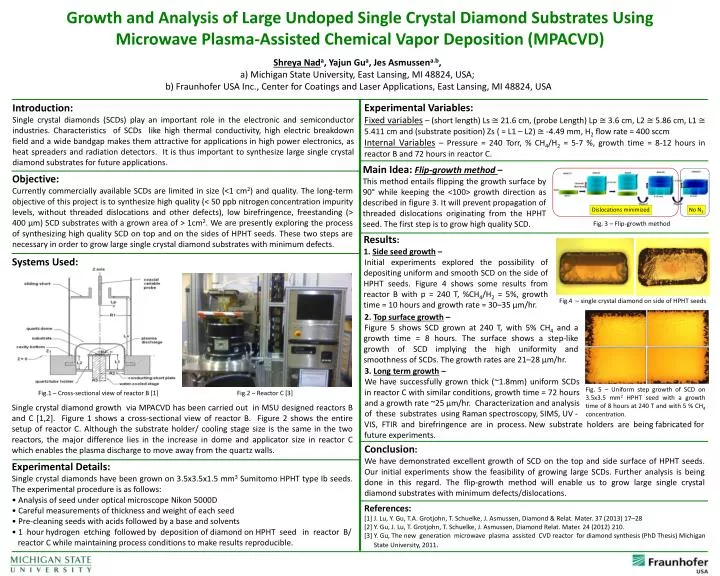
Growth and Analysis of Large Undoped Single Crystal Diamond Substrates Using Microwave Plasma-Assisted Chemical Vapor Deposition (MPACVD). Shreya Nad a , Yajun Gu a , Jes Asmussen a.b , a) Michigan State University, East Lansing, MI 48824, USA;

E N D
Growth and Analysis of Large Undoped Single Crystal Diamond Substrates Using Microwave Plasma-Assisted Chemical Vapor Deposition (MPACVD) • Shreya Nada, YajunGua, JesAsmussena.b, • a) Michigan State University, East Lansing, MI 48824, USA; • b) FraunhoferUSA Inc., Center for Coatings and Laser Applications, East Lansing, MI 48824, USA Dislocations minimized No N2 Experimental Variables: Fixed variables – (short length) Ls ≅ 21.6 cm, (probe Length) Lp ≅ 3.6 cm, L2 ≅ 5.86 cm, L1 ≅ 5.411 cm and (substrate position) Zs ( = L1 – L2) ≅ -4.49 mm, H2 flow rate = 400 sccm Internal Variables– Pressure = 240 Torr, % CH4/H2 = 5-7 %, growth time = 8-12 hours in reactor B and 72 hours in reactor C. Introduction: Single crystal diamonds (SCDs) play an important role in the electronic and semiconductor industries. Characteristics of SCDs like high thermal conductivity, high electric breakdown field and a wide bandgap makes them attractive for applications in high power electronics, as heat spreaders and radiation detectors. It is thus important to synthesize large single crystal diamond substrates for future applications. Main Idea: Flip-growth method – This method entails flipping the growth surface by 90° while keeping the <100> growth direction as described in figure 3. It will prevent propagation of threaded dislocations originating from the HPHT seed. The first step is to grow high quality SCD. Objective: Currently commercially available SCDs are limited in size (<1 cm2) and quality. The long-term objective of this project is to synthesize high quality (< 50 ppb nitrogenconcentration impurity levels, without threaded dislocations and other defects), low birefringence, freestanding (> 400 µm) SCD substrates with a grown area of > 1cm2. We are presently exploring the process of synthesizing high quality SCD on top and on the sides of HPHT seeds. These two steps are necessary in order to grow large single crystal diamond substrates with minimum defects. Fig.4 – single crystal diamond on side of HPHT seeds Results: 1. Side seed growth – Initial experiments explored the possibility of depositing uniform and smooth SCD on the side of HPHT seeds. Figure 4 shows some results from reactor B with p = 240 T, %CH4/H2 = 5%, growth time = 10 hours and growth rate = 30–35 µm/hr. Systems Used: Fig. 3 – Flip-growth method 2. Top surface growth – Figure 5 shows SCD grown at 240 T, with 5% CH4 and a growth time = 8 hours. The surface shows a step-like growth of SCD implying the high uniformity and smoothness of SCDs. The growth rates are 21–28 µm/hr. 3. Long term growth – We have successfully grown thick (~1.8mm) uniform SCDs in reactor C with similar conditions, growth time = 72 hours and a growth rate ~25 µm/hr. Characterization and analysis of these substrates using Raman spectroscopy, SIMS, UV - Single crystal diamond growth via MPACVD has been carried out in MSU designed reactors B and C [1,2]. Figure 1 shows a cross-sectional view of reactor B. Figure 2 shows the entire setup of reactor C. Although the substrate holder/ cooling stage size is the same in the two reactors, the major difference lies in the increase in dome and applicator size in reactor C which enables the plasma discharge to move away from the quartz walls. VIS, FTIR and birefringence are in process. New substrate holders are being fabricated for future experiments. Fig. 5 – Uniform step growth of SCD on 3.5x3.5 mm2 HPHT seed with a growth time of 8 hours at 240 T and with 5 % CH4 concentration. Conclusion: We have demonstrated excellent growth of SCD on the top and side surface of HPHT seeds. Our initial experiments show the feasibility of growing large SCDs. Further analysis is being done in this regard. The flip-growth method will enable us to grow large single crystal diamond substrates with minimum defects/dislocations. Experimental Details: Single crystal diamonds have been grown on 3.5x3.5x1.5 mm3 Sumitomo HPHT type Ib seeds. The experimental procedure is as follows: • Analysis of seed under optical microscope Nikon 5000D • Careful measurements of thickness and weight of each seed • Pre-cleaning seeds with acids followed by a base and solvents • 1 hour hydrogen etching followed by deposition of diamond on HPHT seed in reactor B/ reactor C while maintaining process conditions to make results reproducible. References: [1] J. Lu, Y. Gu, T.A. Grotjohn, T. Schuelke, J. Asmussen, Diamond & Relat. Mater. 37 (2013) 17–28 [2] Y. Gu, J. Lu, T. Grotjohn, T. Schuelke, J. Asmussen, Diamond Relat. Mater. 24 (2012) 210. [3] Y. Gu, The new generation microwave plasma assisted CVD reactor for diamond synthesis (PhD Thesis) Michigan State University, 2011. Fig.1 – Cross-sectional view of reactor B [1] Fig.2 – Reactor C [3]