Download
1 / 2
20 likes | 135 Vues
Electrical Transport in Thin Film Nanostructures Hanno H. Weitering, The University of Tennessee, DMR 0244570.

E N D
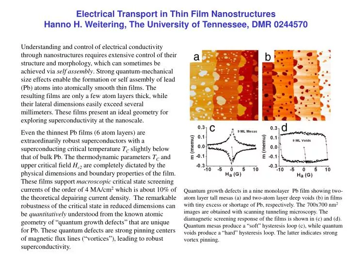
Electrical Transport in Thin Film NanostructuresHanno H. Weitering, The University of Tennessee, DMR 0244570 Understanding and control of electrical conductivity through nanostructures requires extensive control of their structure and morphology, which can sometimes be achieved via self assembly. Strong quantum-mechanical size effects enable the formation or self assembly of lead (Pb) atoms into atomically smooth thin films. The resulting films are only a few atom layers thick, while their lateral dimensions easily exceed several millimeters. These films present an ideal geometry for exploring superconductivity at the nanoscale. Even the thinnest Pb films (6 atom layers) are extraordinarily robust superconductors with a superconducting critical temperature TC slightly below that of bulk Pb. The thermodynamic parameters TC and upper critical field Hc2 are completely dictated by the physical dimensions and boundary properties of the film. These films support macroscopic critical state screening currents of the order of 4 MA/cm2 which is about 10% of the theoretical depairing current density. The remarkable robustness of the critical state in reduced dimensions can be quantitatively understood from the known atomic geometry of “quantum growth defects” that are unique for Pb. These quantum defects are strong pinning centers of magnetic flux lines (“vortices”), leading to robust superconductivity. Quantum growth defects in a nine monolayer Pb film showing two-atom layer tall mesas (a) and two-atom layer deep voids (b) in films with tiny excess or shortage of Pb, respectively. The 700x700 nm2 images are obtained with scanning tunneling microscopy. The diamagnetic screening response of the films is shown in (c) and (d). Quantum mesas produce a “soft” hysteresis loop (c), while quantum voids produce a “hard” hysteresis loop. The latter indicates strong vortex pinning.
Electrical Transport in Thin Film NanostructuresHanno H. Weitering, The University of Tennessee, DMR 0244570 Education: Two graduate students (Murat Ozer and Eun Ju Moon) and one postdoc (Jiandong Guo) contributed to the experimental work. Murat Ozer started his dissertation research in the Fall of 2002 and is expected to obtain his Ph.D. degree in December 2005. His thesis describes formation and superconducting properties of ultrathin lead films. Eun Ju Moon began her thesis research in January 2005. She has build dedicated measurement equipment for in-situ studies of quantum transport in thin film nanostructures. Dr. Jiandong Guo pioneered optical studies of thin film nanostructures. He is leaving the group in October 2005 to become a junior physics professor at the Chinese Academy of Sciences in Beijing. Societal Impact: Nanoscience represents a very promising avenue for future innovations in e.g. the physical sciences, medicine, and information technology. A key requirement for making functional nanodevices is the ability to acquire perfect control of their structure and morphology. A viable way to accomplish this is to exploit quantum mechanical laws while tuning and assembling nano structures. This work represents an important case-study, showing: (1) how quantum mechanics can be used to control the structure and morphology of thin film nanostructures at the atomic level, and (2) how the “quantum engineered morphology” of thin films relates to one of their most appealing functionalities, namely dissipation-free electrical conductivity or “superconductivity.”