Download
1 / 76
1.17k likes | 2.69k Vues
Chapter 2. Basic Semiconductor Physics. 9/12/2008. 2.1 Introduction. Si, GaAs, InP: the published experimental and theoretical values of certain parameters differ considerably from reference to reference. Even worse for less matured materials (e.g., SiC or GaN), alloys and strained layers.

E N D
Chapter 2. Basic Semiconductor Physics 9/12/2008
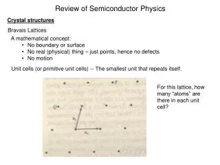
2.1 Introduction • Si, GaAs, InP: the published experimental and theoretical values of certain parameters differ considerably from reference to reference. • Even worse for less matured materials (e.g., SiC or GaN), alloys and strained layers. • The 11 basic semiconductors: the cubic crystal type (Ge, Si, GaAs, AlAs, InAs, InP, GaP), the hexagonal (wurtzite) crystal type (SiC (4H & 6H), GaN, AlN). • A linear interpolation scheme used for approximating material parameters unavailable.
If the material parameters are known for 2 basic binary compounds AC & BC, the composition-dependent material parameter TAxB1-xC(x) of the ternary compound (AxB1-xC) can be estimated by • For a quaternary alloy of composition AxB1-xCyD1-y, • This method is valid only when reliable data for the alloy of interest are not available. • Although numerical device simulation accounts for more physical effects and is often more accurate, analytical approaches nonetheless enjoy great popularity.
2.2 Free-Carrier Densities 2.2.1 Band diagrams and Band structure • Carrier density=the number of carriers/cm3 • Under the thermal equilibrium condition, heat is only energy applied to the semiconductor. • If other types of energy are applied, the equilibrium may be perturbed. nonequilibrium • EG = EC – EV (Energy state ≈ Energy level)
Generation: the electron is lifted to the conduction band, leaving behind an unoccupied state in the valence band. • Recombination: a free electron falls down from the conduction band to the valence band, thereby releasing energy (≥ the bandgap) and filling the hole. • At T=0 K, all allowed states below EF are filled with electrons and all states above EF are empty. • The density of electrons and holes can also be increased by intentionally incorporating impurities (dopants) into the semiconductor.
2.2.2 Carrier Statistics • The density of states (the density of allowed energy states) in the conduction band, N(E): mn,ds: the density-of-states effective electron mass. • The effective density of states in the conduction band, NC, defined as • Therefore,
The probability that E is occupied by an electron is governed by the Fermi-Dirac distribution function f(E): (2-6) At E = EF, f(E) is ½. • The density of electrons at a certain energy: the density of states × the occupation probability = (2-7)
Changing the variable from E to x with (2-10) Fermi integral of the order ½, which unfortunately cannot be solved analytically. • Similarly, the hole density in valence band:
The probability that the energy state is empty, i.e., not occupied by and electron: • After some algebraic manipulations, (2-14)
2.2.3 Approximations for the Carrier Densities • Boltzmann Statistics • For E-EF>3kBT, the exponential term in (2-6) is >>1, (2-16) • Similarly, for EF-E>3kBT • f(E) and fh(E) are called the Boltzmann distribution functions. (2-5)&(2-16)(2-7): (2-18)
Semiconductors with above conditions are nondegenerate. • For degenerate semiconductors (n-type with E-EF<3kBT and p-typewith EF-E<3kBT), the Fermi-Dirac statistics should be used. • Nondegenerate and degenerate semiconductors correspond to lightly and heavily doped materials, respectively. • The electron density = the hole density in an intrinsic semiconductor
Solving the above equations for NC and NV, inserting the results into (2-18), • Under thermal equilibrium mass action law • The charge neutrality is maintained in any semiconductor device regardless of the doping. (Electrons and holes are mobile charges, whereas ionized dopants are fixed.)
Complete Dopant Ionization-Approximation 1 • Assume all donors are ionized in an n-type material and the dopant concentration>>ni n0 ≈ ND, • Similarly, for a p-type, p0 ≈ NA, • Complete Dopant Ionization-Approximation 2 • Low doping or a large intrinsic carrier concentration • In an n-type material, (2-30)
Similarly, for a p-type, • Incomplete Dopant Ionization • The dopant atoms are not 100% ionized. • ND>ND+ in n-type, NA>NA- in p-type. • This occurs either at low temperature or when the dopant’s activation energy is high. • At room temperature, complete ionization can be assumed for most semiconductors, e.g., Si, GaAs, and InGaAs. • In SiC, EDA and EAA are larger than those in the above-mentioned materials, and at room temperature only a portion of the dopants are ionized.
For n-type, the density of ionized donors with EDA and ED is described using the Fermi-like distribution function: ground state degeneracy factor g is added. • The density of ionized donors (i.e., the density of donor states not occupied by an electron) can be: (2-37)
Assuming the electron density ≈ the density of ionized donors, (2-37) (2-38) • Rearranging (2-18) • Insert this into (2-38) and solving a quadratic equation • The density of ionized acceptors: • The probability fA of an acceptor state occupied by an electron can be:
Finally, using (2-19) • Joyce-Dixon Approximation
2.3 Carrier Transport 2.3.1 Introduction • 2 driving forces for carrier transport: electric field and spatial variation of the carrier concentration. • Both driving forces lead to a directional motion of carriers superimposed on the random thermal motion. • To calculate the directional carrier motion and the currents in a semiconductor, classical & nonclassical models can be used. • The classical models assume that variation of E-field in time is sufficiently slow so that the transport properties of carriers (mobility or diffusivity) can follow the changes of the field immediately.
If carriers are exposed to a fast-varying field, they may not be able to adjust their transport properties instantaneously to variations of the field, and carrier mobility and diffusivity may be different from their steady-state values nonstationary • Nonstationary carrier transport can occur in electron devices under both dc and ac bias conditions. • Whether the field acting on the carrier is varying in time or nor is important. • In III-V transistors, nonstationary transport plays an important role, but is much less important in Si transistors. In SiC transistors, it is entirely neglected.
2.3.2 Classical Description of Carrier Transport A. Carrier Drift. • Assume thermal equilibrium for a semiconductor having a spatially homogeneous carrier concentration with no applied E-field. No driving force for directional carrier motion. The carriers not in standstill condition but in continuous motion due to kinetic energy. For electron in the conduction band, wherevth is the thermal velocity, mn* is the conductivity effective electron mass. • The average time btw 2 scattering events is the mean free time and the average distance a carrier travels btw collisions is the mean free path. Fig. 2.5 (a) • Applying V, the E-fields adds a directional component to the random motion of the electron. Fig. 2.5 (b)
The mean electron velocity: vn= -μnE • The directed unilateral motion of carriers caused by E-field is drift velocity. • Similarly, vp= μpE • A change in E-field instantaneously results in a change of the drift velocity.
B. Low-Field Carrier Drift. • The drift velocity is linearly dependent on the field. • The low-field mobilities μ0n and μ0p depend on both the doping concentration and on the temperature. • The dependence of the low-field mobility is modeled empirically
The mobility of minority carriers can be considerably higher than that of majority carriers. • The electron low-field mobilities for Si and GaAs in Fig 2.7 • The low-field electron and hole mobilities of different undoped semiconductors in Fig 2.8
C. High-Field Carrier Drift • v-E characteristics for Si and for semiconductors with similar v-E characteristics can be modeled by the empirical expression • The saturation velocity vsat is temperature-dependent and decreases with increasing temperature. For electrons and holes in Si,
In GaAs or InP, not only can a sublinear slope of the v-E characteristics be observed, but the velocity actually decreases after reaching a peak value at a certain critical field and approaches asymptotically to a saturation value. • Fig 2.11 illustrates the electron population in the lower and upper valleys and the stationary v-E characteristics for GaAs.
D. Drift Current Densities • The drift current density JDr is described by the product of the density, the charge, and the drift velocity of the drifting carriers. • Under low-field conditions where v = μ0E holds, • The total drift current density JDr = JDr,n +JDr,p.
E. Carrier Diffusion and Diffusion Current Densities • In a nonuniform carrier distribution, carriers tend to move from higher carrier concentration to lower carrier concentration. diffusion • At x = x0, the probability that an electron moves to the left is the same as the probability that it moves to the right. • The average rate P1 of electrons flowing from x1 toward x0 and crossing the plane x = x0 is
Approximating the concentration at x1, • Analogously, the average rate of electrons flowing from x-1 toward x0 is • The net rate P of electrons crossing the plane at x0 in +x direction is the difference btw P-1 and P1, • Introducing the electron diffusion coefficient Dn=vthΔx, • The electron diffusion current density JDi,n can be obtained from the net rate of electron diffusion by multiplying P with the charge of an electron, i.e., by –q, as
Similarly, • JDi = JDi,n+ JDi,p • Driving force for a diffusion current is the gradient of the carrier concentration, whereas the driving force for a drift current is the electric field. • The main difference btw these driving forces is that the field acts directly on the carriers and give rise to a directional motion of every carrier in the sample, whereas an individual carrier does not feel any force from a carrier concentration gradient. • A relationship btw mobility and diffusion coefficient Einstein relation: (2-70)
F. Alternative Expressions for the Current Density • Since , • Similarly, • Therefore, the general driving force for a current is the gradient of the Fermi level, and it is impossible to identify from whether this driving force is caused by a field or a gradient of the carrier concentration.
2.3.3 Nonclassical Description of Carrier Transport • The basic assumption of the classical description of carrier drift a sudden change of the field results in an immediate change of carrier drift velocity: Not correct!! • According to classical mechanics, a particle with a certain mass cannot change its velocity instantaneously because of inertia, even if the driving force for the motion does. • Carriers possess a certain mass (the effective mass) and need a certain transition time to change their kinetic energy and their velocity after a sudden variation of the field. • The behavior of carriers during the transition period is called carrier dynamics or nonstationary carrier transport. • Such a transport was first investigated using MonteCarlo Simulation for Si and GaAs.
It can also be described easily by the relaxation time approximation (RTA). The heart of the RTA is the energy and momentum balance equations, for a homogeneous semiconductor: where τEand τp: the energy-dependent effective relaxation times for carrier energy and momentum, E0: the carrier energy at thermal equilibrium (E = 0), m*: the conductivity effective electron mass (the effective mass related to transport phenomena), m*×v : momentum P of the carrier. • The balance btw the amount of energy and momentum that carriers gained from the applied field, and the energy and momentum loss caused by scattering. The effects of all different scattering events are combined in τEand τp
Stationary v-E, E-E, and m*-E are needed to simulate nonstationary transport. • Let us consider an n-type GaAs sample, at time t, the electron possess E(t), P(t) and m*(t) and travel with v(t). Now assume that during the small time interval Δt after t the applied field changes from E(t) to E(t+Δt). The evolution of the electron velocity: • Calculate τE(t+Δt) and τP(t+Δt) by assuming stationary conditions (d/dt=0) • Calculate the electron energy and momentum at t+Δt. For this, the balance equations are discretized.
Set Est(t+Δt) = E(t+Δt) and deduce the new stationary values Est(t+Δt), vst(t+Δt) and mst*(t+Δt) from Fig 2.15 • Calculate the electron velocity v(t+Δt) from • Increase the time by another Δt and proceed with step 1.
Velocity overshoot: when a large field is applied, the electron velocity reaches a much higher peak than that predicted by the stationary v-E characteristics.
In Fig.2.18, the field is in –x direction and is the driving force for a drift current. This drift tendency is in the opposite direction of the diffusion tendency. With no bias applied to the pn junction, the diffusion and drift tendencies compensate each other, and no net carrier flow occurs. • The electron affinity χ is the energy difference btw the vacuum level and the conduction band edge. • The energy barrier btw the p- and n-type regions is the same for the conduction and valence bands built-in voltage Vbi of the pn junction. • Derivation of Vbi: When no external voltage is applied, no net current flows across the junction. (2-84)
Rearranging (2-84) and applying Einstein relation (2-70) • Integrating across the space-charge region (-xp ~ xn), • To find the thickness of the space-charge region, using Poisson equation, where ε = ε0εr
In the space-charge region on the p-type side, simplified to • Applying the boundary condition, i.e., E-field = 0 at x=-xp, (2-89) • Similarly, on the n-type side, (2-90)
Integrating (2-89) & (2-90) gives the potential distribution, using B.C. (φ=0 at x=-xp, φ=Vbi at x=xn), • Because the potential in a pn junction is continuous, the thickness of the space-charge region under the thermal equilibrium (no voltage is applied)