Download
1 / 17
220 likes | 380 Vues
Unit 8 Combinational Circuit Design and Simulation Using Gates. Ku-Yaw Chang canseco@mail.dyu.edu.tw Assistant Professor, Department of Computer Science and Information Engineering Da-Yeh University. Contents. 8.1 Review of Combinational Circuit Design

E N D
Unit 8Combinational Circuit Design and Simulation Using Gates Ku-Yaw Chang canseco@mail.dyu.edu.tw Assistant Professor, Department of Computer Science and Information Engineering Da-Yeh University
Contents 8.1 Review of Combinational Circuit Design 8.2 Design Circuits with Limited Gate Fan-In 8.3 Gate Delays and Timing Diagrams 8.4 Hazards in Combinational Logic 8.5 Simulation and Testing of Logic Circuits Fundamentals of Logic Design
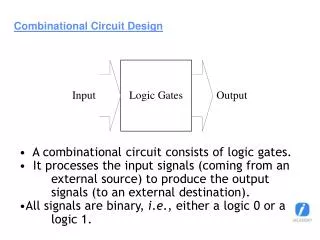
Combinational v.s. Sequential • Combinational circuit • Output values depend only on the present value of the inputs (not on the past values) • Sequential circuit • Output values depend on both present and past input values • Composed of • A combinational circuit • Added memory elements Fundamentals of Logic Design
Combinational Circuit Design • First step • Set up a truth table • n input variables -> 2n rows • Don’t care condition • A given combination never occurs • Next step • Derive simplified expression • Karnaugh maps • Quine-McCluskey Fundamentals of Logic Design
Combinational Circuit Design • Third step • Manipulate simplified expressions into proper form • Depending on the type of gates to be used in realizing the circuit • Factoring or multiplying out • Levels • Gates • Gate inputs Fundamentals of Logic Design
Combinational Circuit Design • Minimum sum-of-products • AND-OR, NAND-NAND, OR-NAND, NOR-OR Fundamentals of Logic Design
Combinational Circuit Design • Minimum product-of-sums • OR-AND, NOR-NOR, AND-NOR, NAND-AND Fundamentals of Logic Design
Contents 8.1 Review of Combinational Circuit Design 8.2 Design Circuits with Limited Gate Fan-In 8.3 Gate Delays and Timing Diagrams 8.4 Hazards in Combinational Logic 8.5 Simulation and Testing of Logic Circuits Fundamentals of Logic Design
Limited Gate Fan-in • The maximum number of inputs on each gate (or the fan-in) is limited. • Factoring maybe necessary Fundamentals of Logic Design
Example • Realize f(a,b,c,d) = ∑m(0, 3, 4, 5, 8, 9, 10, 14, 15)using 3-input NOR gates. Fundamentals of Logic Design
Karnaugh Map ab ab 00 01 11 10 00 01 11 10 cd cd 00011110 00011110 Fundamentals of Logic Design
Karnaugh Map f ’ = a’b’c’d + ab’cd + abc’ + a’bc + a’cd’ ab 00 01 11 10 cd 00011110 Fundamentals of Logic Design
Resulting NOR-gate circuit • f ’ = a’b’c’d + ab’cd + abc’ + a’bc + a’cd’ = b’d (a’c’ + ac) + a’c (b + d’) + abc’ • f = [b+d’+(a+c)(a’+c’)] [a+c’+b’d] [a’+b’+c] Fundamentals of Logic Design
Example • Realize the functions, using only 2-input NAND gates and inverters. • f1 = ∑m(0, 2, 3, 4, 5) • f2 = ∑m(0, 2, 3, 4, 7) • f3 = ∑m(1, 2, 6, 7) Fundamentals of Logic Design
Karnaugh Map • f1 = b’c’ + ab’ + a’b • f2 = b’c’ + bc + a’b • f3 = a’b’c + ab + bc’ Fundamentals of Logic Design
Factoring • To introduce common terms wherever possible • f1 = b’c’ + ab’ + a’b = b’(a+c’) + a’b • f2 = b’c’ + bc + a’b = b(a’+c) + b’c’ or (b’+c)(b+c’) + a’b • f3 = a’b’c + ab + bc’ = a’b’c + b(a+c’) • Eliminating 3-input gate from f3 • a’b’c = a’(b’c) = a’(b+c’)’ Fundamentals of Logic Design
Realization Fundamentals of Logic Design