Download
1 / 78
850 likes | 1.58k Vues
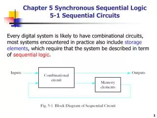
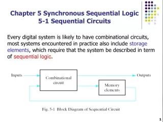
Chapter 5 Sequential Logic Sequential Logic Combinational circuit outputs depend on present inputs. Sequential circuit outputs depend on present inputs and the state of the memory elements. Outputs Inputs Combinational Circuit Memory Sequential Circuit

E N D
Chapter 5 Sequential Logic
Sequential Logic Combinational circuit outputs depend on present inputs. Sequential circuit outputs depend on present inputs and the state of the memory elements. Outputs Inputs Combinational Circuit Memory Sequential Circuit
Flip-Flop - a storage (memory) element. A flip-flop circuit has two outputs, one normal form and one complemented. It may have one or two inputs, depending on type. Clock, preset and clear functions may also be present. One flip-flop stores one binary bit. R Q S R Q Q 1 0 1 0 0 0 1 0 0 1 0 1 0 0 0 1 1 1 0 0 Q S NOR X Y Z 0 0 1 0 1 0 1 0 0 1 1 0 1) Logic 1 on S sets Q to 1. 2) Logic 1 on R resets Q to 0. 3) Logic 1 on both S, R produce an indeterminate result.
Clocked RS Flip-Flop Q S R Q ( T+1) R 0 0 0 0 0 0 1 0 0 1 0 1 0 1 1 Indeterm 1 0 0 1 1 0 1 0 1 1 0 1 1 1 1 Indeterm Q CP Q S Characteristic Table S Q CP R Q
S SR Q(t + 1) = S + RQ SR= 0 Q 0 0 d 1 1 0 d 1 Q SR must equal 0 so that S and R cannot both be 1 simultaneously R Q = present state Q(t + 1) = next state Indeterminate states can be considered as don’t cares since either a 1 or a 0 may result after S and R both equal 1.
D Flip-Flop D Q CP Q S Q D Q(t+1) 0 0 0 0 1 1 1 0 0 1 1 1 D Q CP Q D 1 Characteristic Table Q 1 Q( t + 1) = D
Q Q JK Flip-Flop R K CP S J
Q J K Q ( t+1) J Q 0 0 0 0 0 0 1 0 0 1 0 1 0 1 1 1 1 0 0 1 1 0 1 0 1 1 0 1 1 1 1 0 CP K Q J Characteristic Table 0 0 1 1 Q(t+1) = J Q + KQ Q 1 0 0 1 K
Q Q T Flip-Flop R T CP S
Q T Q(t + 1) 0 0 0 0 1 1 1 0 1 1 1 0 T Q CP Q T 1 Q ( t + 1) = T Q + T Q Q 1
Triggering of Flip-Flop * Synchronous: behavior can be defined from the knowledge of signals at discrete instants of time. A master clock is used, only change during a clock pulse. * Asynchronous: behavior depends on the order in which input signals change. Can be changed at any time. Level Triggering: Flip-Flop sensitive to pulse duration Edge Triggering: Flip-Flop sensitive to pulse transition (solves feedback timing problems) 1 0 Positive edge Negative edge
Master-Slave Flip-Flops: Contains two separate flip-flops Q S S Q S Q CP CP Master Slave R Q R Q Q R
Problem: Instability occurs if output of memory elements (FF’s) are changing while output of combinational circuit that go to the Flip-Flop inputs are being sampled by the clock pulse. Inputs FF CP Output Comb. Logic Propagation delay from Flip-Flop input to output must be greater then clock pulse duration.
CP S Input Y Output Q Output state change occurs on the negative clock transition.
Direct Inputs Preset J Q PR CP K Q CL Clear
State Diagrams State: The condition (values) stored in the flip-flops of a sequential circuit. Present State: The condition of the flip-flops prior to a clock pulse. Next State: Condition of the flip-flops after a clock pulse state a 1/0 1/1 transition between states which occurs with a clock pulse. 0/0 b d 1/0 0/0 0/1 X/Y x= input which causes transition. y = output during present state. 0/0 c 1/0
State Table Contains the same information as a state diagram Next State Output X = 0 X = 1 X = 0 X = 1 Present state a 0 0 c b 0 0 b 0 1 c b 1 0 c 1 0 d c 0 0 d 1 1 c a 0 1 In general, a state table for m flip-flops will have 2m rows, one for each state. The next state and output section will have 2n columns each for n inputs. External outputs can be taken from flip-flop output or from logic gates. If there are no logic gates for output, the output columns can be deleted. The output is then read directly from the present state of the flip-flops.
State Reduction Goal: reduce the number of flip-flops in a sequential circuit. Next State Output X = 0 X = 1 X = 0 X = 1 Present state a a b 0 0 b c d 0 0 c a d 0 0 d e f 0 1 e a f 0 1 f g f 0 1 g a f 0 1 Equivalent states = same input gives the same output for each state and the transitions go to the same state. In example above state g = state e . . . . .
State Reduction . . . . . and state f = state d. Next State Output X = 0 X = 1 X = 0 X = 1 Present state a a b 0 0 b c d 0 0 c a d 0 0 d e f 0 1 e a f 0 1 f g f 0 1 g a f 0 1 e
State Reduction . . . . . and state f = state d. Next State Output X = 0 X = 1 X = 0 X = 1 Present state a a b 0 0 b c d 0 0 c a d 0 0 d e f 0 1 e a f 0 1 f g f 0 1 g a f 0 1 d d e
State Assignment Some state assignment schemes can reduce the combinational portion of a sequential circuit. However, there are no state assignment techniques which guarantee minimization. Suggestion: 1) For counters use the sequence of binary numbers for state assignments. 2) Otherwise, make arbitrary assignments.
Flip-Flop Excitation Tables Characteristic tables define next state - when the input and present state are known . Excitation tables define the input conditions required to make a desired transition from a known present state to a a desired next state. Q S R Q ( T+1) Q Q(t + 1) S R 0 0 0 0 0 0 1 0 0 1 0 1 0 1 1 Indeterm 1 0 0 1 1 0 1 0 1 1 0 1 1 1 1 Indeterm 0 0 0 d 0 1 1 0 1 0 0 1 1 1 d 0 SR Excitation Table SR Characteristic Table
Q J K Q ( t+1) 0 0 0 0 0 0 1 0 0 1 0 1 0 1 1 1 1 0 0 1 1 0 1 0 1 1 0 1 1 1 1 0 Q Q(t + 1) J K 0 0 0 d 0 1 1 d 1 0 d 1 1 1 d 0 JK Excitation Table JK Characteristic Table Q Q(t + 1) D Q D Q(t + 1) 0 0 0 0 1 1 1 0 0 1 1 1 0 0 0 0 1 1 1 0 0 1 1 1 D Excitation Table D Characteristic Table
Sequential Design Process Goal: obtain a logic diagram or list of Boolean functions which describe a sequential circuit meeting the design specification. 1) Write a word description. Draw a state diagram. 2) Construct a state table. 3) Perform state reduction. 4) Make state assignments. 5) Determine number of ff required and assign a letter to each. 6) Select type of ff to use. 7) Construct circuit excitation and output tables. 8) Reduce Boolean functions. 9) Draw the logic diagram.
Example Design a circuit to implement the following state diagram. 0/1 a 1/1 1/0 0/0 1/1 b d 1/1 0/0 c 0/1
2) Conduct a state table. Next State Output X = 0 X = 1 X = 0 X = 1 Present state a a b 1 1 b c b 0 1 c c d 1 1 d d a 0 0 3) Perform state reduction. None possible.
4) Make state assignments. a = 0 0 b = 0 1 c = 1 0 d = 1 1 5) Determine number of flip-flops required 4 states required 2 flip-flops (2n = 4) 6) Select flip-flop type. Choose T. (TA, TB)
7) Construct excitation and output tables. Inputs of combinational circuit Output of combinational circuit Present State Input Next State FF inputs Output A B X A B TA TB Z 0 0 0 0 0 0 0 1 0 0 1 0 1 0 1 1 0 1 0 1 0 1 1 0 0 1 1 0 1 0 0 1 1 0 0 1 0 0 0 1 1 0 1 1 1 0 1 1 1 1 0 1 1 0 0 0 1 1 1 0 0 1 1 0 a a b b c c d d
Q Q(t + 1) T Using: 0 0 0 0 1 1 1 0 1 1 1 0 8) Reduce Boolean Functions. B 0 0 0 1 TA = A B X + A B X A 0 0 1 0 X
B 0 1 0 1 TB = B X + AX + A B X A 0 1 1 0 X B 1 1 1 0 Z = B + A X A 1 1 0 0 X
9) Draw the logic diagram. T Q T Q A B Q Q TA A A TB B B X Input Z Output Conbinational Circuit
A B X TA A B X B X TB A X A X Z B
Example Design a sequential circuit using the following state table: Next State Output X = 0 X = 1 X = 0 X = 1 Present state 0 0 0 0 0 1 0 0 1 0 1 0 0 0 0 1 0 0 1 1 1 0 0 0 0 0 1 1 0 0 1 1 0 0 0 0 1 0 0 1 0 1 1 0 0 0 1 1 0 1 0 0 1 1 0 0 0 1 1 1 0 1 1 1 3 flip-flop are requires for 5 states. There will be 3 numbered states (000, 110, 111). Letter the ff A,b, C. Construct an excitation table for RS ff.
Present State Input Next State Flip-Flop Inputs Output A B C X A B C S A R A S B R B S C R C Y 0 0 0 0 d d d d d d d d d d 0 0 0 1 d d d d d d d d d d 0 0 1 0 0 0 1 0 d 0 d d 0 0 0 0 1 1 0 1 0 0 d 1 0 0 1 0 0 1 0 0 0 1 1 0 d d 0 1 0 0 0 1 0 1 1 0 0 1 0 0 1 0 d 0 0 1 1 0 0 0 1 0 d 0 1 d 0 0 0 1 1 1 1 0 0 1 0 0 1 0 1 0 1 0 0 0 1 0 1 d 0 0 d 1 0 0 1 0 0 1 1 0 0 d 0 0 d 0 d 1 1 0 1 0 0 0 1 0 1 0 d d 0 0 1 0 1 1 1 0 0 d 0 0 d 0 1 1 1 1 0 0 d d d d d d d d d d 1 1 0 1 d d d d d d d d d d 1 1 1 0 d d d d d d d d d d 1 1 1 1 d d d d d d d d d d
Use the SR excitation table to complete the circuit excitation table: Q Q(t +1) S R 0 0 0 d 0 1 1 0 1 0 0 1 1 1 d 0 Reduce Boolean function: C CX AB d d 0 0 0 1 1 0 d d d d d d d 0 SA = BX B A X
C CX AB Others SB = A B X RB = B C + B X S C = X R C = X Y = A X d d d d d 0 0 d d d d d 0 0 0 1 RA = CX B A X
Draw the logic diagram: Y Output SA A S Q X Input A CP RA A R Q SB B S Q B RB CP R Q B SC C S Q B CP RC R Q CP
Don’t Care States 0/0 0 0 1 0/0 ?? 0/0 0 0 0 1/0 1 0 1 0 1 1 0 1 0 0/0 1/0 1/0 ?? 0/0 1 1 0 1 0 0 1/1 1 1 1 ??
Don’t Care States • What about don’t care states? • Self-Correcting: all unused states eventually lead to valid • states. (some designs may specify self-correcting in one clock • pulse.) • Self-starting: initial state on power up is specified. Usually a • master reset input is used. It is customary to provide a master- • reset input whose purpose is to initialize the states of all • flip-flops in the system. Typically, the master reset is a signal • applied to all flip-flops asynchronously before master-reset • signal, but some may be set to 1. • Q: What if, because of a noise signal the circuit finds itself in • an invalid state? In that case it is necessary to ensure that the • circuit eventually goes into one of the valid states so it can resume • normal operation.
Don’t Care States • It was stated previously that unused states in a sequential • circuit can be treated as don’t-care conditions. • Once the circuit is designed, the m flip-flops in the system can • be in any of 2 possible states. • Some of these states were taken as don’t cares conditions. • The circuit muse be investigated to determine the effect of these • unused states. The next state from invalid sates can be determined.
0/0 0/0 0 0 1 0/0 0/0 0/0 0 0 0 1/0 1 0 1 1/0 0 1 1 0 1 0 0/0 1/0 1/0 0/0 1 1 0 0/0 1 0 0 1/1 1/1 1 1 1
Design Problem 0/0 0 0 1 0/0 1/1 1/0 1 0 0 0 1 1 0/0 0/0 1/1 0 1 0 1/1 0/0 1/1 0 0 0
Example Problem: Design with T Flip-Flops Present State Input Next State Flip-Flop Inputs Output A B C X A B C TA TB TC 0 0 0 0 0 1 1 0 1 1 0 0 0 0 1 1 0 0 1 0 0 1 0 0 1 0 0 0 1 0 0 0 0 0 0 1 1 1 0 0 1 0 1 1 0 1 0 0 0 1 0 0 0 0 0 0 1 0 1 0 0 0 0 1 0 1 0 1 1 0 0 0 1 0 1 0 0 0 1 1 1 0 1 0 0 0 1 1 1 0 0 0 0 1 0 1 1 0 0 1 0 0 1 0 1 1 1 1 1 0 1 0 1 1 0 1 1 1 0 1 1 0 1 1 1 1 1 1 Need 3 Flip-Flops to Get 5 States Unused States
Don’t Care States ?? 0/0 0 0 1 0/0 1/1 1 1 1 1/0 1 0 0 0 1 1 0/0 0/0 1/1 1 1 0 0 1 0 1/1 0/0 1 0 1 1/1 0 0 0
C C CX CX AB AB 0 1 1 0 0 0 0 0 d d d d 1 1 d d 1 0 0 0 0 1 0 1 d d d d 1 1 d d B B A A TA = A + BX X X TB = A + B C X + B C X + B C X C CX C CX AB AB 1 0 1 0 0 0 1 0 d d d d 0 1 d d 0 1 1 0 0 1 1 0 d d d d 0 0 d d A A Z= AX TC = AX + CX + A B C X X X
To Gates Prob 6-20 CONTD A TA T B X Q Z A Q A X A To Gates B B C X To Gates TB T B C Q X Q B C B X To Gates To Gates A A C TC T Q X Q C X *Note Clock Pulse is assumed To Gates C
Prob CONTINUED Now, we must analyze circuit to confirm that unused states are in fact “Don’t Cares” Analyzes Procedure is: 1) Start w/Logic Diagram 2) Formulate FF input Equations 3) Derive next state equations using FF characteristics EQ. 4) Formulate transition table (state table w/binary #’s) 5) Formulate state diagram. 1) Logic Diagram on previous Page 2) TA = A + BX QA = A TB = A + BC X + B C X + B C X QB = B TC = AX + CX + A B C X QC = C
3) T F-F Char. EQ: Q(t +1) = TQ + TQ A = (A + B X) A + (A + BX) A A B X + [ A (B + X) ] A A B X + (A B + A X) A A B X B = (A + B C X + B C X + B C X) B + (A + B C X + B C X + B C X) B AB + B C X + [ A (B + C + X) (B + C + X) ( B + C + X) ] B AB + B C X + [ BA (B + BC + BX) (BC + BX) (BC + BX) ] AB + B C X + [B A + A B C + A B X) (BC + BX) (BC + BX) AB + B C X + [A B C + A B X + A B C + A B X + A B C X + A B X) (B C + B X) AB + B C X + A B C X + A B C X CX C AB 1 B = A B + A C X + A B C X 1 1 B A 1 1 1 1 X
1 C = (AX + CX + A B C X) C + ( A X + C X + A B C X) C A C X + A B C X +[ (A + X) (C + X) (A + B + C + X) ] C A C X + A B C X + (C A + C X) (C X) (C A + C B + C + C X) A C X + A B C X + ( C A X + CX) ( CA + CB + C + CX) A C X + A B C X + C A X B + C A X + C X A + C X B + CX A C X + A B C X + C A X ( B + 1) + C X A + C X B + C X A C X + A B C X + A C X + A CX + B C X + C X CX C AB 1 C = CX + A C X + A B X 1 1 B 1 A 1 1 X
4) Present State Input Next State Output A B C X A B C 0 0 0 0 0 1 1 0 0 0 0 1 1 0 0 1 0 0 1 0 0 0 1 0 0 0 1 1 1 0 0 1 0 1 0 0 0 1 0 0 0 1 0 1 0 0 0 1 0 1 1 0 0 0 1 0 0 1 1 1 0 1 0 1 1 0 0 0 0 1 0 0 1 0 0 1 0 1 1 0 1 0 1 0 0 1 1 0 1 0 1 1 0 1 0 0 1 1 0 0 0 0 0 0 1 1 0 1 0 0 1 0 1 1 1 0 0 0 1 0 1 1 1 1 0 0 0 0