Download

1 / 15
160 likes | 260 Vues
Combinational Logic Design. Combinatorial. Logic. Circuit. m Boolean Inputs. n Boolean Outputs. Combinational Circuits. A combinational logic circuit has: A set of m Boolean inputs, A set of n Boolean outputs

E N D
Combinatorial Logic Circuit m Boolean Inputs n Boolean Outputs Combinational Circuits • A combinational logic circuit has: • A set of m Boolean inputs, • A set of n Boolean outputs • n switching functions, each mapping the 2m input combinations to an output such that the current output depends only on the current input values A block diagram
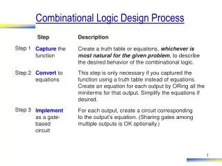
Design Procedure Steps • Specification • Formulation • Optimization • Technology Mapping: • AND, OR, and NOT; NAND; NOR • Verification • Manual • Simulation
Design Procedure • Specification • Write a specification for the circuit if one is not already available • Formulation • Derive a truth table or initial Boolean equations that define the required relationships between the inputs and outputs, if not in the specification • Apply hierarchical design if appropriate (more later)
Design Procedure • Optimization • Apply 2-level and multiple-level optimization • Draw a logic diagram (or provide a netlist ) for the resulting circuit using ANDs, ORs, and inverters
Design Procedure • Technology Mapping • Map the logic diagram or netlist to the implementation technology selected • Verification • Verify the correctness of the final design manually or using simulation
Hierarchical Design • Objective: To control the complexity of each function which is mapping inputs to outputs • Decompose the function into smaller pieces called blocks • Decompose each block’s function into smaller blocks, repeating as necessary until all blocks are small enough • Any block not decomposed is called a primitive block • The collection of all blocks including the decomposed ones is a hierarchy
Design Hierarchy • Just like with a large software program, to design a large chip you need a hierarchy • Divide and Conquer • Block is equivalent to object
Example: 9-input even parity checker • Design a 9-input function to check even parity for byte • Chapter 2: Use odd function circuit to check even parity
We know how to design an XOR Y X • A NAND only implementation is: X Y
The blocks that must be designed Components in Design
9-input parity tree (continued) • Top Level: 9 inputs, one output • 2nd Level: Four 3-bit odd funcions in two levels • 3rd Level: Two 2-bit exclusive-OR functions • Primitive block, XOR gate: Four 2-input NAND gates • Design requires {4 X (2 X 4)} = 32 2-input NAND gates
Top Down Design • Ideally you specify top level of design and work your way down • Real life isn’t that way • Work some at top • Build/test some low-level blocks • Go back to top level • Just like real software programs • Big projects (like Pentium) done with architecture and levels of simulators