Download
1 / 39
570 likes | 2.13k Vues
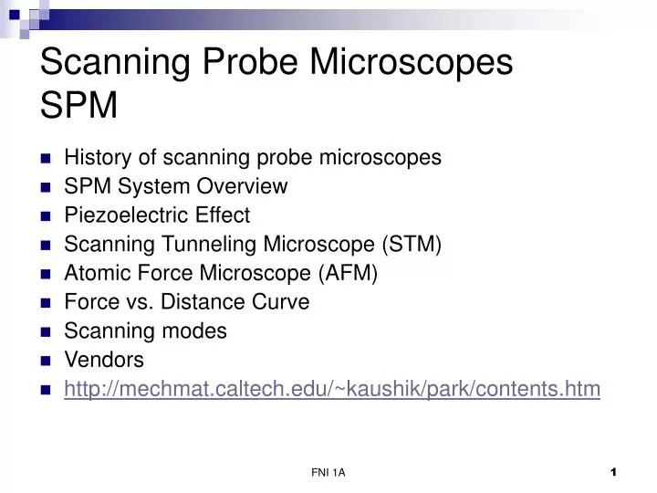
Scanning Probe Microscopes SPM History of scanning probe microscopes SPM System Overview Piezoelectric Effect Scanning Tunneling Microscope (STM) Atomic Force Microscope (AFM) Force vs. Distance Curve Scanning modes Vendors http://mechmat.caltech.edu/~kaushik/park/contents.htm

E N D
Scanning Probe MicroscopesSPM • History of scanning probe microscopes • SPM System Overview • Piezoelectric Effect • Scanning Tunneling Microscope (STM) • Atomic Force Microscope (AFM) • Force vs. Distance Curve • Scanning modes • Vendors • http://mechmat.caltech.edu/~kaushik/park/contents.htm FNI 1A
History of Scanning Probe Microscopes • Phonograph record http://www.nanoworld.org/english/museum.html FNI 1A
History of Scanning Probe Microscopes • 1929 • Gustev Schmalz • Stylus profiler FNI 1A
History of Scanning Probe Microscopes • 1971 • Russel Young • Topographiner • A non-contact stylus profiler FNI 1A
History of Scanning Probe Microscopes • 1981 • Gerd Binnig & Heinrich Rohrer • Scanning Tunneling Microscope (STM) FNI 1A
History of Scanning Probe Microscopes • Atomic Force Microscope (AFM/SFM) • Gerd Binnig, Calvin Quate & Christoph Gerber • 1986 FNI 1A
SPM System Overview FNI 1A
SPM Scan Head Non Contact AFM STM Force Modulation AFM Contact AFM Lateral Force Microscopy Laser should be switched on to operate FNI 1A
SPM Scan Head Second: Adjust detector alignment until red lights are out and green light is on. First: Adjust cantilever alignment so laser is aligned on the cantilever FNI 1A
Pre-Mounted AFM Probe Tip FNI 1A
Cartridges AFM Cartridge STM Cartridge FNI 1A
Digital Voltmeters FNI 1A
Photodetector Top = 1+2 1 2 Bottom = 3+4 3 4 A = 1+3 B = 2+4 LFM records Top-Bottom and should be minimized A+B Should be Maximized A-B Should be Minimized FNI 1A
Scanning Tunneling Microscope • Applications • System Components • Tube scanner • Piezoelectric effect • Theory of operation • Operating modes • Advantages & Disadvantages FNI 1A
Applications • High resolution images at atomic resolution. • Ability to manipulate individual atoms. • http://www.almaden.ibm.com/vis/stm/gallery.html FNI 1A
STM System Components FNI 1A
Piezoelectric tube scanner Piezoelectric materials are used to create a tube scanner. This forms one of the basic components of scanning probe microscopes. These can be used to manipulate an object in three dimensions under electronic control. FNI 1A
Piezoelectric Effect Certain materials exhibit what is called the piezoelectric effect. (Demo) This is an effect where changing the size of an object results in a voltage being generated by the object. Conversely when a voltage is applied to a piezoelectric object then the size of the object changes. FNI 1A
Piezoelectric Effect PZT: Lead zirconium titanate is one of the most common piezoelectric materials. Piezoelectric materials have an asymmetric unit cell like a dipole. If these crystals are grown in the presence of a strong electric field then the crystal grains will align and the piezoelectric effect is created. FNI 1A
Unit Cell with Dipole The central atom is displaced resulting in a unit cell with a dipole moment. Cubic T > Tc Tetragonal T < Tc FNI 1A
Piezoelectric EffectCrystal grains structure Not grown in an electric field Random orientation Grown in an electric field Unit cell dipoles align FNI 1A
STM Theory of operation Tunneling Current FNI 1A
Operating modes • Constant height mode • Current changes exponentially • Requires a smooth surface • Constant current mode • Beware of insulators FNI 1A
STM Advantages & Disadvantages • Advantages • Able to obtain very high resolution images of conductors and semiconductors. • Probe tips can be made out of wire. • Inexpensive to purchase ~ $10,000 • Disadvantages • Will not work with insulators. • If there are insulating materials present on the sample you can crash the tip. • Often need to be used under vacuum. FNI 1A
Scanning Tunneling Microscope • Applications • System Components • Tube scanner • Piezoelectric effect • Theory of operation • Operating modes • Advantages & Disadvantages FNI 1A
Atomic Force Microscope • System Components • Force vs. Distance • Performance & Images • Scanning Modes & Probe Tips • Vendors FNI 1A
AFM System Components Demo FNI 1A
Force vs. Distance FNI 1A
Performance • The piezoelectric tubes have a movement resolution of 1 nm/volt. • Magnifications of 5,000,000x can be achieved. • Resolution of 10 pm • Can operate in air and under liquids • Atomic force microscopes can be used on many different surfaces. • AFM is a versatile and easy to use tool. • Images http://www.nanoscience.com/ • AFM Activity • WS 13 FNI 1A
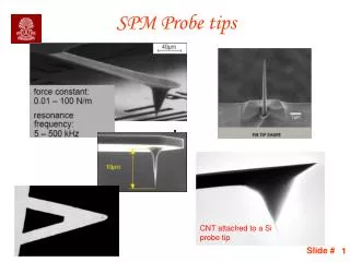
Scanning Modes and Probe Tips • Standard probe tips • High resolution probe tips • Magnetic force microscopy • Frictional force microscopy/Lateral force microscopy • Elasticity/hardness measurements/Force modulation microscopy • Scanning Capacitance • Thermal scanning microscopy – two different metals/ thermo couple • Near-field Scanning Optical Microscopy/Light funnel • Piezoelectric cantilever • Electrostatic force microscopy • Dip pen nanolithography • Surface oxidation • Many different companies make probe tips for scanning microscopes. FNI 1A
Veeco http://www.veeco.com/ JEOL http://www.jeol.com/ Nanoscience Instruments http://www.nanoscience.com/ Asylum Research http://www.asylumresearch.com/ JPK Instruments http://www.jpk.com/index2.htm Molecular Imaging http://www.molec.com/ Nanofactory Instruments http://www.nanofactory.com/ Nanotec Electronica http://www.nanotec.es/ NT-MDT http://www.ntmdt.ru/ Quesant http://www.quesant.com/ WITec http://www.witec.de/ Pacific Nanotechnology http://www.pacificnanotech.com/ Nanoics Imaging http://www.nanonics.co.il/main/ Schaefer-TEC http://www.schaefer-tec.com/ Windsor Scientific http://www.windsor-ltd.co.uk/ LOT Oriel Ltd http://www.lot-oriel.com/uk/htm/all/home01.php Atomic Force http://www.atomicforce.de/ Mikro Masch http://www.spmtips.com/ Surface Imaging Systems http://www.sis-gmbh.com/ Physik Instrumente http://www.polytecpi.com/ Accurion http://www.accurion.com/ Advanced Surface Microscopy http://www.asmicro.com/ Hysitron http://www.hysitron.com/ Infinitesima http://www.infinitesima.com/ Nanograph Systems http://www.nanographsystems.co.uk/ Nanonis http://www.nanonis.com/nanonis/avs/home/index.html PSIA http://www.advancedspm.com/ Triple-O Microscopy http://www.triple-o.de/ Bioforce http://www.bioforcelab.com/ Scanning Probe Microscope Vendors FNI 1A
Scanning Probe Microscopes • System Components • Force vs. Distance • Performance & Images • Scanning Modes & Probe Tips • Vendors FNI 1A
Links • http://stm2.nrl.navy.mil/how-afm/how-afm.html • http://www.ikm.uni-karlsruhe.de/forschung/pzt_webseiten/eng/basics/ferro_main_eng.html • http://cst-www.nrl.navy.mil/lattice/struk/pzt_t.html • http://www.chembio.uoguelph.ca/educmat/chm729/STMpage/stmconc.htm • http://www.2spi.com/catalog.html FNI 1A