Download
1 / 2
20 likes | 154 Vues
Integrating GaAs on Virtual Ge-on-Si Substrates Sang M . Han, University of New Mexico, DMR 0907112.

E N D
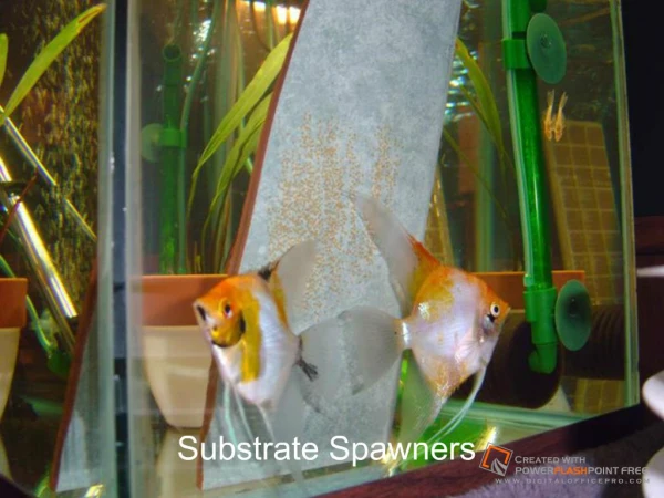
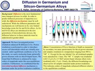
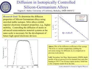
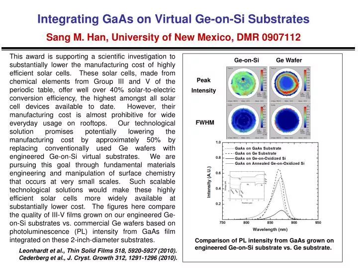
Integrating GaAs on Virtual Ge-on-Si SubstratesSang M. Han, University of New Mexico, DMR 0907112 This award is supporting a scientific investigation to substantially lower the manufacturing cost of highly efficient solar cells. These solar cells, made from chemical elements from Group III and V of the periodic table, offer well over 40% solar-to-electric conversion efficiency, the highest amongst all solar cell devices available to date. However, their manufacturing cost is almost prohibitive for wide everyday usage on rooftops. Our technological solution promises potentially lowering the manufacturing cost by approximately 50% by replacing conventionally used Ge wafers with engineered Ge-on-Si virtual substrates. We are pursuing this goal through fundamental materials engineering and manipulation of surface chemistry that occurs at very small scales. Such scalable technological solutions would make these highly efficient solar cells more widely available at substantially lower cost. The figures here compare the quality of III-V films grown on our engineered Ge-on-Si substrates vs. commercial Ge wafers based on photoluminescence (PL) intensity from GaAs film integrated on these 2-inch-diameter substrates. Ge-on-Si Ge Wafer Peak Intensity FWHM Comparison of PL intensity from GaAs grown on engineered Ge-on-Si substrate vs. Ge substrate. Leonhardt et al., Thin Solid Films 518, 5920-5927 (2010). Cederberg et al., J. Cryst. Growth 312, 1291-1296 (2010).
Outreach to Math & Science Charter High School Students Sang M. Han, University of New Mexico, DMR 0907112 Outreach is an important component of integrative research education. In particular, high school students’ early introduction to science and engineering can significantly influence their decision to pursue a career in these areas. To maximize this impact, Darin Leonhardt, a Graduate Research Assistant in the Han group at UNM, participated in a Science Fair held at Albuquerque Institute for Math and Science (AIMS). AIMS is a charter school that specializes in math and science education from 3rd grade to high school level. As a judge, Darin provided high school student participants with detailed feedback on their projects and how they can improve, encouraging their efforts to engage in science and engineering. He also led class discussions on engineering ethics at AIMS. He engaged the students in several case studies that required critical thinking related to different ethical dilemmas. The discussions were very lively and served to illustrate the multifaceted nature of ethics and how researchers apply ethical guidelines to steer their work.