Download
1 / 25
250 likes | 370 Vues
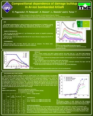
Soltan Institute for Nuclear Studies. Compositional dependence of damage buildup in Ar - ion bombarded Al x Ga 1-x N. Karolina Danuta Pągowska. Outline. 1. Energy loss of ions in solids, collision cascade 2. Ion implanter 3. FET 4. RBS and channeling

E N D
Soltan Institute for Nuclear Studies Compositional dependence of damage buildup in Ar - ion bombarded AlxGa1-xN Karolina Danuta Pągowska
Outline 1. Energy loss of ions in solids, collision cascade 2. Ion implanter 3. FET 4. RBS and channeling 5. Channeling spectra for ion bombarded GaN 6. Multi-step damage accumulation in irradiated crystals 7. Summary
0 1 2 3 4 5 6 Depth/ µm Energy - Depth – Relation for 1.5 MeV He–ions in Si Rp = 5.21 µm
Energy loss of ions in solids He ions Ar ions Energy loss He ions Ar ions Ionization dEe/dx Displace- ments dEn/dx Ion velocity ~ (Energy)1/2
Accelerator Wobbler Magnetic separator Magnetic lenses Target chamber Extraction Ion source Ion implanter
Ion beam Mask Sample Ion implantation in compound semiconductors and their heterostructures in usually performed for: • Doping • Insulating region formation (patterned implantation)
Ion beam Mask Si substrate Field – Effect Transistor (FET)
SiO2 Si SOI – Silicon On Insulator
x0 x0 Energy Depth 4He, 2 MeV Si SiO2 x0 - O - Si Principles of Rutherford Backscattering Spectrometry Yield Detector
Defect analysis using ion channeling Short summary of HRXRD superlattice analysis
Schematic representation of the MSDA model a Low fluence Stage 1 Structure C Structure B Structure A Structure A b Medium fluence Stage 2 Structure B Structure C A B Structure A Structure B Structure A c High fluence Stage 3 Structure C B C Structure B Structure B Structure A A B Structure C Structure A
Three-step accumulation For GaN fd1=6 sig1=0.77 fd2=68.5 sig2=0.0398 x2=12.5 fd3=100 sig3=0.008 x3=400
Two-step accumulation For AlGaN fd1=6 sig1=0.86 fd2=54 sig2=0.015 x2=5
For AlNfd1=7sig1=0.245fd2=63.5sig2=0.02x2=10 Two-step accumulation