Download
1 / 56
1.14k likes | 2.48k Vues
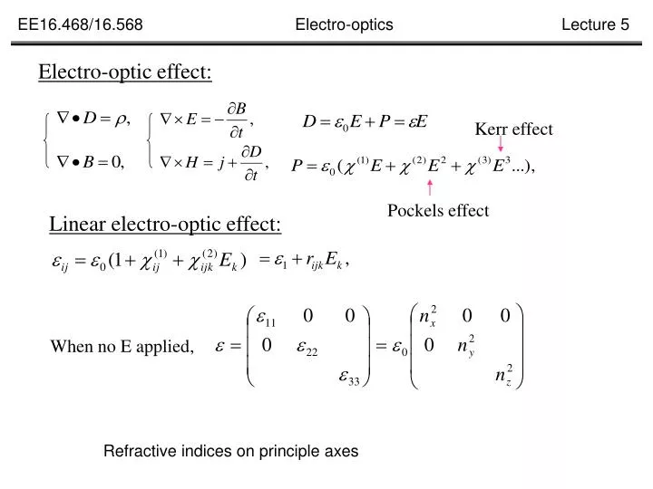
Electro-optic effect:. Kerr effect. Pockels effect. Linear electro-optic effect:. When no E applied,. Refractive indices on principle axes. Refractive index ellipsoid:. When no electric field applied,. Refractive index ellipsoid. n z. n y. n x. Refractive index ellipsoid:. Generally,.

E N D
Electro-optic effect: Kerr effect Pockels effect Linear electro-optic effect: When no E applied, Refractive indices on principle axes
Refractive index ellipsoid: When no electric field applied, Refractive index ellipsoid nz ny nx
Refractive index ellipsoid: Generally, is a 3x3 tensor, = -1 or= -1 When electric field applied, 3x3x3 tensor, 27 components No EO effect for crystal with central symmetry, why? Why? + z z z x x y y y x x z y -
j i = 1 2 3 1 6 5 1 2 6 2 4 5 4 3 3
Take LiNbO3 as an example: Z cut TM polarization TE polarization
Take LiNbO3 Intensity modulator Z cut TM polarization
Take LiNbO3 Intensity modulator Z cut TM polarization Linear region Frequency double region
Operating characteristics • Modulation depth • Bandwidth: the highest frequency the modulator can operate, R and C • Insertion loss (dB):
Power consumption: P/f, f: bandwidth for a channel waveguide, assuming the E filed is uniform, C ~ 0.4pF Take LiNbO3 as an example: P/f ~ 2µW/MHz
Power consumption: P/f, f: bandwidth for a bulk EO modulators, assuming the E filed is uniform, z C ~ 3pF Take LiNbO3 as an example: P/f ~ 2W/MHz
Phase modulator: Phase shift due to the applied voltage: Examples:
+ - z z
Polarization modulator: x y Phase shift due to the applied voltage:
Polarization modulator: W x y Ax Ay Phase difference due to the applied voltage:
Polarization modulator: Phase difference due to the applied voltage: W x y Ax Ax When = /2, Ay Ay Ax Ax When = , Ay Ay
TE-TM converter: Phase Shift (degree) Bias (V)
Quantum Key Distribution (QKD) Bennett and Brassard 1984 protocol Proc. IEEE Int. Conf. Computers, Systems and Signal Processing, 1984, pp. 175–179. Single photon JUSTIN MULLINS, IEEE SPECTRUM, p. 40, May 2002
Quantum Key Distribution (QKD) Bennett and Brassard 1984 protocol Proc. IEEE Int. Conf. Computers, Systems and Signal Processing, 1984, pp. 175–179. JUSTIN MULLINS, IEEE SPECTRUM, p. 40, May 2002
Quantum Key Distribution (QKD) W. T. Buttler, etal. Physical Review A, Vol 57, 1998, pp. 2379-2382
Receiver: Bob QKD Links Transmitter: Alice QKD Links Receiver: Bob Integrated QKD Receiver
Phase Shift (degree) Bias (V)
EO Polymer poling Poling of polymer materials, contact poling and corona poling:
V Heating/Cooling block Needle V Electrode Poling Electrode EO polymer Film Buffer Layer Buffer Layer Heating/Cooling block Advantages: • Lower voltage ~ 800V • Good film quality • Uniform poling voltage • Easy control of poling voltage • Select poling area
I-V curve during poling: • Poling voltage : 900V • EO coefficient ~ 22pm/V
TM-pass waveguide Polarizer TM input TE input
Directional coupler: 1 3 For A1(0) = A1, A2(0) =0 A1(z) A2(z) Un-connected port 4
Directional coupler: 1 3 For A1(0) = A1, A2(0) =0 A1(z) A2(z) Un-connected port 4
1 3 A1(z) A2(z) Un-connected port 4 For A1(0) = A1, A2(0) =0
Directional coupler: 1 3 For A1(0) = A1, A2(0) =0 A1(z) A2(z) Un-connected port 4
B A + V0 Z0 VL Vg(t) Vi ZL l z = - l z = 0 - V0 Traveling-wave electrodes: 1 3 For A1(0) = A1, A2(0) =0 A1(z) A2(z) Un-connected port 4 For high-speed electrode using transmission lines: - ZL Z0 = + ZL Z0
B A + V0 Z0 VL Vg(t) Vi ZL l z = - l z = 0 - V0 |V(z)| + 2|V0| - -3/4 -/2 -/4 Standing waves for impedance mismatching: - ZL Z0 = + ZL Z0 Standing waves Cancelled
B A |V(z)| + V0 + |V0| Z0 VL Vg(t) Vi ZL - -3/4 -/2 -/4 l z = - l z = 0 - V0 Traveling waves for impedance matching: - ZL Z0 = + ZL Z0 traveling waves
Applicationsof Kerr effect : • Self-phase modulation • Self-Focusing
Acoustic-optic Modulators • Bragg condition:
Doppler shift Angle mismatch
Acoustic –optics devices • Modulator Bandwidth: • Beam Scanner Number of resolvable spots:
Acoustic –optics devices • Free space inter-connector • Isolator
Light propagation in anisotropic crystals Optical axises o light no
Light propagation in anisotropic crystals Optical axis o light no ne