Download
1 / 18
180 likes | 184 Vues
Explore the potential of graphene transistors as a solution to the short channel effects in transistors and memory. Discover the advantages of graphene memory, such as increased storage capacity, lower power consumption, and resistance to extreme environments.

E N D
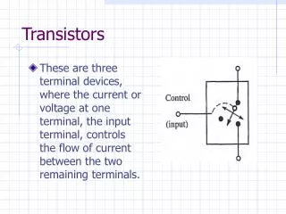
THE PROBLEM • SHORT CHANNEL EFFECTS :- • NARROW CHANNEL EFFECTS :- Reduction in saturation mode drain current. Variation in Carrier velocity. Modification of threshold voltage. Sub-threshold current. Punch through.
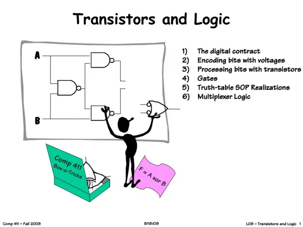
THE SOLUTION • GRAPHENE TRANSISTORS • Graphene is a one-atom-thick planar sheet of sp2 bonded carbon atoms that are densely packed in a honeycomb crystal lattice. • A tiny jolt of electricity (+5v) can 'break' a strip of graphene just ten atoms thick; another jolt (-5v) restores it to normal.
Thus a strip of graphite only 10 atoms thick can serve as the basic element in a new type of memory. • The new switches can be controlled by two terminals instead of three, as in current chips.
Development of switch • The process of creating two-terminal graphite stripes starts with chemical vapor deposition (CVD) of graphene onto silicon. Using photo-lithography, strips of chromium are deposited on top of the graphene, exposed graphene is removed, and then the chromium is dissolved, leaving clean, microscopic stripes of graphene on silicon. With platinum contacts added via lithography to the ends of the stripes, the graphene becomes addressable bits of memory.
Working • The gate electrode is separated from the graphene by a thin layer of silicon dioxide dielectric. The application of –5 volts to the gate electrode causes the conductance of the graphene to decrease by more than six orders of magnitude and essentially cutting off the flow of current. When the voltage is reversed to +5 V, the conductance returns to what it had been before the voltage was applied.
The electric field causes a hydroxyl molecule to attach to the graphene, changing it to graphene oxide. The hydroxyl is borrowed from the silicon dioxide dielectric that sits on top of the graphene.
Advantages 1. Graphene memory would increase the amount of storage in a two-dimensional array by a factor of five as individual bits could be made smaller than 10 nanometers, compared to the 45-nanometer circuitry in today’s flash memory chips.
2. The new switches can be controlled by two terminals instead of three, as in current chips. Two-terminal capability makes three-dimensional memory practical as graphene arrays can be stacked, multiplying a chip’s capacity with every layer.
3. The on-off power ratio (the amount of current a circuit holds when it's on, as opposed to off) of graphene memory is huge. Its a million-to-one. While the on/off ratios of phase-change materials are generally in the 10-100 region. The transistors currently used in computer chips have on/off ratios of 10,000 - 100,000
4. Being essentially a mechanical device, such chips will consume virtually no power while keeping data intact – much the same way today’s e-book readers keep the image of a page visible even when the power is off. 5. It has the ability to operate with as little as three volts
6. Graphene memory seems impervious to a wide temperature range, having been tested from minus 75 to more than 200 degrees Celsius with no discernable effect. Better still, tests show it to be impervious to radiation, making it suitable for extreme environments.
Disadvantages 1. The switching of graphene memory is not fast enough yet to be used in a logic circuit. 2. It is not yet shown that it will work for the millions of cycles a memory device would require.
3. A way to deposit graphene on large scale instead of small pieces is still needed to be developed. It can take a long time before its implementation in actual circuit.