Download
1 / 1
20 likes | 161 Vues
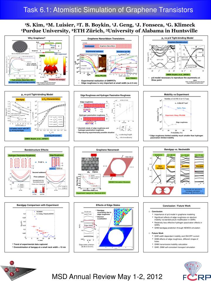
Task 6.1: Atomistic Simulation of Graphene Transistors. G. Bulk. S. D. 1 S. Kim, 2 M. Luisier, 3 T. B. Boykin, 1 J. Geng, 1 J. Fonseca, 1 G. Klimeck 1 Purdue University, 2 ETH Zürich, 3 University of Alabama in Huntsville. Efield. G. Graphene. S. D. AGNR 13.

E N D
Task 6.1: Atomistic Simulation of Graphene Transistors G Bulk S D 1S. Kim, 2M. Luisier, 3T. B. Boykin, 1J. Geng, 1J. Fonseca, 1G. Klimeck 1Purdue University, 2ETH Zürich, 3University of Alabama in Huntsville Efield G Graphene S D AGNR 13 pz vs p/d Tight-binding Model Why Graphene? Graphene Nanoribbon Transistors AGNR 12 Graphene Bandstructure Graphene Nanoribbon Confinement Experimental realization Simulation (pz-TB) http://en.wikipedia.org/wiki/Graphene DIBL suppressed NEMO5 Akturk, JAP2008 Shishir, JPCM2009 OMEN: Boykin, et al., JAP2011 Wang, PRL2008 • p/d model necessary to reproduce the asymmetry at Dirac point Betti, ITED2011 Problem: No bandgap Frank schwierz, Nature Nano. 2010 • Experimental realization of GNRFETs • Edge roughness is very important at small width (w<2.5 nm) OMEN- https://engineering.purdue.edu/gekcogrp/software-projects/omen/ NEMO5- https://engineering.purdue.edu/gekcogrp/software-projects/nemo5/ Excellent high field transport/mobility pz vs p/d Tight-binding Model Mobility vs Experiment Edge Roughness and Hydrogen Passivation Roughness Vd Edge roughness n~ 0.95x10¹³/cm2 S D Hydro. Pass. C Id H Vd Hydrogen passivation roughness Experiment: Wang, PRL2008 D S Edge roughness Id • Atomistic study of edge roughness and hydrogen passivation roughness • Reproducing experimentally possible situation p/d better match with DFT pz-wrong bandgap 2 • Edge roughness limited mobility much smaller than hydrogen passivation limited mobllity pz-wrong off-current OMEN: Boykin, et al., JAP2011 Bandgap vs. Neckwidth Bandstructure Effects Graphene Nanomesh Graphene 33 nm w = 26 nm w = 11 nm w = 19 nm Edge Roughness Hydrogen Passivation Roughness 138x138 uc P=50 % C H C Zero bandgap Bandgap Bandgap Bandgap H AGNR-12 AGNR-13 Second subband 33 nm First subband NEMO5 Simulation Structure Ef Ef Flat bands are ignored in bandgap calculation (crieterion: dE/dk<0.53 eV ) w Experiment: Liang et al., NanoLett 2010 Bandgap Comparison with Experiment Effects of Edge States Conclusion / Future Work • Bandgap uncertainty due to edge roughness • Electron Localization • Conclusion • Importance of p/d model in graphene modeling • Significant effects of edge roughness on electron mobility via bandstructure modification in GNRs • Relatively less effective hydrogen passivation effects in GNRs • GNM bandgap prediction through NEMO5 simulation • Future Work • GNR width dependent mobility and ON/OFF-current • GNM effects of edge roughness, different shape of holes • GNM transmission/mobility calculation • GNR, GNM self-consistent transport simulation D=24 nm w=9.7 nm Edge states Eg Γ Γ • Trend of experimental data captured • Overestimation of bangap at a small neck width < 10 nm Edge states criterion: dE/dk<0.53 eV