Download
1 / 32
370 likes | 441 Vues
Quantum Well Infrared Detector. Jie Zhang, Win-Ching Hung. Department of Electrical and Computer Engineering. Outline. Introduction Quantum Well Infrared Photodetectors QWIP Focal Plane Arrays Applications Summary. Atmospheric transmittance. Force Enhancement. Space Control.

E N D
Quantum Well Infrared Detector Jie Zhang, Win-Ching Hung Department of Electrical and Computer Engineering
Outline • Introduction • Quantum Well Infrared Photodetectors • QWIP Focal Plane Arrays • Applications • Summary
Force Enhancement Space Control Space-Based Missions Surveillance Protection of Assets Counter Enemy Capabilities
Detecting Infrared Radiation • HgCdTe semiconductors • Schottky barriers on Si • SiGe heterojunctions • AlGaAs MQWs • GaInSb strain layer superlattices • High T superconductors • Silicon Bolometers • ……..
Thermal Detectors Photodetectors Intrinsic Extrinsic Photoemissive Quantum Well Classes of IR Detectors
Outline • Introduction • Quantum Well Infrared Photodetectors • QWIP Focal Plane Arrays • Applications • Summary
CB CB CB kT kT kT VB VB VB Semiconductors METAL Conduction Band close to Valence Band. Electrons easily excited out of VB. Electrons in CB free to move. INSULATOR Conduction Band far from Valence Band. Electrons not easily excited out of VB. SEMICONDUCTOR Conduction Band relatively close to Valence Band. Electrons can be excited out of VB under certain conditions.
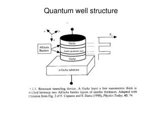
A B A 2-D Quantum Confinement Bulk Semiconductors Epitaxial Layers A B A 50 nm 5 nm 50 nm Conduction Bands Conduction Band Discrete Energy Levels Valence Band Valence Bands “Quantum Well”
Multiple Quantum Wells Bulk Semiconductor A Bulk Semiconductor B Grown atom-by-atom in an MBE machine (Molecular Beam Epitaxy) Semiconductor Heterostructure A multi-quantum well layer structure used as a detector is called a “QWIP” (Quantum Well Infrared Photodetector) Quantum Well Bandstructure
H g C d T e Q u a n t u m W e l l 1 - x x C B C B B o u n d S t a t e V B V B Physics Quasi-Bound State Energy Energy
Design: Key Aspects • 1-D arrays with the growth direction normal to the layers. • Vertical quantized quantum levels. • Horizontal planes exhibit a uniform energy state which allows electrons to move freely within the plane. • All electrons in a horizontal plane have the same transition energy • Only photons with energies corresponding to the selected energy gaps can be detected. • Well-depth can be altered by changing the properties of the layered materials. • Stacking wells allows for higher absorptions
AlGaAs GaAs AlGaAs GaAs AlGaAs GaAs/ AlGaAs GaAs AlGaAs GaAs Incidence angle
Optical Coupling (1) • Light waves that strike the layers perpendicularly show no excitation • Options: • 45 degree wedge • Bend the light inside the detectors with a roughed mirror on the back to scatter normal light. • The mirror can be roughed randomly or periodically
Intersubband Absorption • Transitions between energy within same band • Intersubband transition energy • Transition energy inversely proportional to square of well-thickness. • Wide range wavelength • Short-wave infrared (SWIR) λ~ 2μm • Medium-wave infrared (MWIR) λ~ 4μm • Long-wave infrared (LWIR) λ~10μm • Very long-wave infrared (VWIR) λ>14μm
Transitions • Bound to Bound • Bound to Continuum • Bound to Quasi- Bound
Bound-to-Continuum • Excited bound state is situated in the contunuum • Photoexcited eletrons escape without tunneling • Low bias voltage • Low dark current
Bound-to-Bound • Photo-excitation to another bound state within same energy band • Excited carriers escape out of well by tunneling
QWIPs Vs. HgCdTe • HgCdTe has higher absorption coefficient and lower thermal emission, especially at higher temperatures (>75K) • QWIPs show better capabilities as FPAs: High impedance, fast response time, long integration time, and low powe consumption • QWIPs have a greater potential in the VLWIR FPA operation with multi-color detection
Outline • Introduction • Quantum Well Infrared Photodetectors • QWIP Focal Plane Arrays • Applications • Summary
Fabrication 1. Epitaxial growth of QWIP structure 2. Processing of the QWIP array 3. Fabrication of ROIC (readout integrated circuit) 4. Processing of indium bumps 5. Hybridization flip-chip bonding 6. Mounting and wire bonding
QWIP Camera • MWQs • Stacks of 50 n-doped GaAs well with Al0.3Ga0.7As barriers • Uses bound to quasi-bound transitions • Used low operating bias which resulted in only a 1.4% QE • Used periodic mirror etching • Pixel size: 23x23 square micrometers • Cooled with closed-cycle Sterling Cooler • Consumes <45W • Operational temperature up to 70K 12-640x512 pixel arrays on a 3 inch GaAs wafer
Outline • Introduction • Quantum Well Infrared Photodetectors • QWIP Focal Plane Arrays • Applications • Summary
Automotive Industry • Weather Forecasting • Electronics • Infrared target detection • Astronomy Industrial Space Medical Military (MWIR)&(LWIR) (MWIR,LWIR)&VLWIR) (LWIR) Applications of IR Detector Arrays
Application of VLWIR Detectors Deep Space Astronomy Atmospheric pollution monitoring Early detection of long range missiles
Conclusion • QWIPs vs. HgCdTe detectors - Better imaging applications - Easy fabrication and low cost • Physics of QWIPs - Quantum wells - Intersubband transition • Fabrication and characterization • Applications • Chanllenges
Disadvantages Requires low temperatures to operate. As with all photoconductors, noise is inevitable.


![[Nonuniform primary photocurrent spreading in quantum well infrared photoconductors]](https://cdn2.slideserve.com/5143935/nonuniform-primary-photocurrent-spreading-in-quantum-well-infrared-photoconductors-dt.jpg)