Download
1 / 25
430 likes | 1.26k Vues
Infrared, Self Assembled InAs/ GaAs Quantum Dot, Photodetectors. Michiel C. Donker. June 23, 2005. R u G. VLWIR > 12 μ m < 0.10 eV. SWIR = 0.7 - 3 μ m 1.77 - 0.41eV. LWIR = 7 - 12 μ m 0.18 - 0.10 eV. MWIR = 3 - 7 μ m 0.41 - 0.18 eV. Infrared Light.

E N D
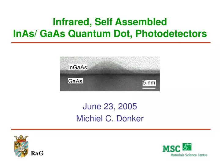
Infrared, Self Assembled InAs/ GaAs Quantum Dot, Photodetectors Michiel C. Donker June 23, 2005 RuG
VLWIR > 12 μm < 0.10 eV SWIR = 0.7 - 3 μm 1.77 - 0.41eV LWIR = 7 - 12 μm 0.18 - 0.10 eV MWIR = 3 - 7 μm 0.41 - 0.18 eV Infrared Light Infrared
LWIR IR Detector Applications • Medicine • Medicine • Astronomy • Astronomy • Defense • Defense • Environment • Environment 8.5 μm 0.15 eV
Content • Introduction • Quantum Dots • Device Fabrication • Electronic Structure • Characterisation and Performance • Conclusion
IR IR HgCdTe Detectors • Hg1-xCdxTe • Wavelength 0.7- 25 μm • High detectivity • Difficult to process 0.0495 - 1.77 eV Hole Vbias =1.0 V • Photo Current HgCdTe • Dark Current Electron
z cross section GaAs InAs InAs Quantum Well 2D 50 nm Conduction band cross section GaAs: Eg= 1.52 eV E cross section GaAs InAs GaAs GaAs InAs: Eg =0.36 eV InAs GaAs Valence band InAs Quantum Dot 0D z Quantum Wire 1D Quantum Confinement InAs Bulk 3D
Density of States Bulk Quantum Well Quantum Wire Quantum Dot g(E)= density of states
< Ψi I r I Ψj > = 0 111 211 x=0 x=L Quantum Dot: Particle in a Box • Infinite potential barrier • Ψ~ sin(nπx/ Lx) sin(mπy/ Ly) sin(lπz/ Lz) • Selection rules: 1-D
InAs GaAs Heavely n- doped GaAs InAs Heavely n- doped GaAs Self Assembled Quantum Dots • Host: GaAs 5.653 Å • Quantum Dot: InAs 5.867 Å • Stranski- Krastanov growth GaAs
IR IR GaAs conduction band Wetting Layer 128 meV d 121 meV 115 meV IR 63 meV p 100010 56 meV s 000 0 meV 930 meV 0 meV h 000 31 meV h 100010 55 meV h 110 57 meV h 200 61 meV h020 Wetting Layer GaAs 3D valence band Electronic Structure • Lens shaped QD’s • Pyrimidal QD’s S.Sauvage et al. C.R. Physique 4, p1133 (2003)
Conduction band Conduction Band edge S P transition S P transition S wetting layer, conduction band Characterisation • Intersubband: absorption e e Δn=odd non zero Δn=even zero In plane as well as normal incidence absorption S.Sauvage et al. C.R. Physique 4, p1133 (2003)
IR Vbias Dark and Photo Current • Thermionic emission • Tunneling • Thermally assisted tunneling • Thermal generation e/ h pair GaAs conduction band Energy InAs wetting layer • Wetting layer • Conduction band • Bound state z direction
phonon (lattice vibration) e-e scattering e-h scattering phonon phonon IR Capture Probability Carrier relaxation processes: GaAs • recombination D ΔE= h c/ λcut off P S The more electrons in a QD, the more charge. E GaAs InAs z
77 K Vbias (V) H.C. Liu, Opto Electronic Review 11, p.1-5 (2003) y z · xy x z S.Sauvage et al. C.R. Physique 4, p1133 (2003) Dark and Photo Current • Thermal generation • Tunneling • Number of electrons per QD • QD density • Number of QD layers • Capture probability Dark 20 K • Angle of incidence • Shape and size • Absorption cross section • Vbias D.Pang et el. Appl. Phys. Lett. 75, p. 2719 (1999)
- η = quantum efficiency = # generated electrons by photons # incident photons τ carrier lifetime - g = gain == # carriers through device # generated carriers by photons τcarrier transit time Iphotocurrent Poptical power e η g h v Responsivity and Detectivity • Responsivity (mA/ W) == • Detectivity (cm Hz1/2/ W) = signal to noise ratio • Background photon noise • Photo electron noise; detectable carrier η, not detectable (1- η) • Receiver circuit noise
Responsivity (A/ W) 165 eV Wavelength (μm) Responsivity and Detectivity Iphotocurrent • Responsivity (mA/ W) = Poptical power L. Jiang et al. Appl. Phys. Lett. 82, p.1986 (2003) • Detectivity (cm Hz1/2/ W) = signal to noise ratio 77 K Vbias= -2.0 V QD density = 1.2 x 10¹⁰ Size 26 nm 6 nm D = 3.6 x 1010 cm Hz1/2/ W
xy Vbias z Conclusion • QD: D = 3.6 x 1010 cm Hz1/2/ W • HdCdTe: D = 2.2 x 1012 cm Hz1/2/ W • # electrons per dot • dot density • dot size and shape • spacing thickness • transport direction J.Philips et al. Encyclopedia of Nanoscience and Nanotechnology, 9 p. 131 (2004)
Acknowledgements Paul van Loosdrecht Quantum Well Camera
< Ψi I r I Ψj > = 0 Δn=odd, on the same axis 000 100 100 010 100 200 000 200 X X <1 | z | 2>= (16/9π2)/L <1 | z | 4>= (4/45π2)/L x=0 x=L Questions • Infinite potential barrier • Ψ~ sin(nπx/ L) sin(mπy/ L) sin(lπz/ L) • Selection rules: • Fermi golden rule:
Intersubband selection rules: e e Δn=odd strong Δn=even zero Interband selection rules: h e Δn=0 strong Δn=0 odd weak Δn=0 even zero H 000 E 000 Questions • Interband: Photo Luminescense • Intersubband: Absorption S.Sauvage et al. C.R. Physique 4, p1133 (2003)
| <n0| k·p |j0> |2 En(0) – Ej (0) Questions • D= R AΔf / Inoise • H= Hk·p + Hstrain + Vconfining potential • En (k) = En (0) + h2k2/2m + h2/m2Σ’ n= band index
Vbias Questions GaAs GaAs AlGaAs AlGaAs InAs E z
Questions L. Jiang et al. APL 82, p.1986 (2003)
Questions S.F. Tang et al. APL 78, p. 2428 (2001)


![[0-11]](https://cdn1.slideserve.com/3481506/slide1-dt.jpg)