Download
1 / 9
90 likes | 195 Vues
Semiconducting Light-Emitting Devices. James A. Johnson 16 December 2006. Direct Semiconductors. Indirect Semiconductors. Semiconducting Materials . Conduction band exists directly “above” valence band.

E N D
Semiconducting Light-Emitting Devices James A. Johnson 16 December 2006
Direct Semiconductors Indirect Semiconductors Semiconducting Materials • Conduction band exists directly “above” valence band. • Electrons and holes may recombine without diverting energy to maintaining conservation of momentum. • Excess energy resulting from recombination is converted to photons. • Prime example of direct semiconductor material is Gallium Arsenide (GaAs) • Conduction band and valence bands are offset by some vector k. • In order for electrons and holes to recombine, they must travel across the k-space. • Traveling across k-space requires conservation of energy and momentum. • Energy that would have become photons in direct semiconductor is used for travel. • Conservation of momentum is attained by production of phonons. • Prime example of indirect semiconductor material is Silicon (Si)
Light-Emitting Device Structure • Four layers in the basic Light-emitting device structure: Substrate, n-type material, active region, p-type material. • Substrate is typically constructed from n-type Si or Sapphire. • n-type layer is typically a GaAs or GaN based alloy. • Active region is typically p-type GaAs or GaN. • p-type layer is typically a p+-type GaAs or GaN based alloy. • Common gallium based alloys include: • Indium Gallium Arsenide - InGaAs • Aluminum Gallium Arsenide - AlGaAs • Indium Gallium Nitride - InGaN • Aluminum Gallium Nitride - AlGaN
Basic Light-Emitting Device Types Edge Light-Emitting Device • Edge emitting device structure lends itself to use current fabrication technologies with little modification. • Double heterojunction structure provides greatest efficiency by creating waveguides for new photons. • Laser diodes have highly polished surfaces for focused light emission and roughened surfaces to minimize reflection.
Basic Light-Emitting Device Types • Improving Efficiency in the Edge Light-Emitting Device • Homojunction – Low internal reflection. Photon energy is absorbed and lost in the surrounding semiconductors. • Single Heterojunction – Improves efficiency of light emission. Energy is still lost in the homogenous semiconductor layer. • Double Heterojunction – Greatest efficiency. Both semiconductor layers reflect photons and guide them to the edge of the structure.
Basic Light-Emitting Device Types Surface Light-Emitting Device • Surface emitting device is fabricated using current technologies, but process is more complicated as all layers do not have uniform areas. • Multiple wavelengths may be constructed in the same device. • Light with longer wavelengths are constructed deeper in the device. • All electrical contacts are placed on the same side; rather than “sandwiching” the device as observed in the edge emitter. • Allows better control of directionality of emitted light.
Edge Emitting Devices It is difficult to construct 2-dimensional arrays of edge-emitting devices. Packaging must be used to improve directionality of light emission. Surface Emitting Devices Fabrication requires etching of portions of layers to place electrical contacts. Due to placement of the electrical contacts, it is difficult to guarantee uniform current in each layer of the device. Challenges with Light-Emitting Devices
Light-Emitting Device Applications and Packaging • A Sample of Applications • PCB Components • Traffic Lights • Motor Vehicle Lights • Railroad Crossing Bars • Flashlights • Remote Controls • Christmas Decorations • Fiber Optic Transmitters • Laser Pointers • Packaging depends greatly upon the application of the device. • Traditional through-hole and SMD components use reflective cups to deflect emitted light. • Devices are being redesigned to accommodate more efficient packaging such as epitaxial lift-off. • Surface emitting devices are being designed to have lenses fabricated on the emitter area to focus or disperse light and to interface with fiber optic cables.
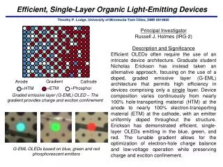
Emerging Light-Emitting Devices • LED’s using quantum dots. • This LED combines the edge emitting structure with the efficiency of surface emitting devices. • A layer of CdSe/ZnS core-shell nanocrystal quantum dots (NQD’s) is placed on top of the light-emitting device structure. • NQD’s have exceptional luminescent properties, but are difficult to energize. • Wavelength may be tuned at time of fabrication based on the size of the NQD’s. • NQD’s are energized when recombination energy is transferred to the quantum dots through a process called Förster Energy Transfer. • This offers a practical solution to the problem of general lighting sources suitable to illuminate objects from large cities to optical microscopes due to efficiency, stability, expected longevity, and potential ease of fabrication.