Download
1 / 14
140 likes | 143 Vues
595 Presentation Day Schedule Change!. Due to EMS construction, Final Presentations will be conducted Friday, May 9 in EMS-E250 Proposed Team Schedule 8:00-9:50 AM: Team 1 10:00 – 11:50AM: Team 2 12:30 – 2:20PM: Team 3 2:30 – 4:20PM: Team 4 4:30 – 6:20PM: Team 5

E N D
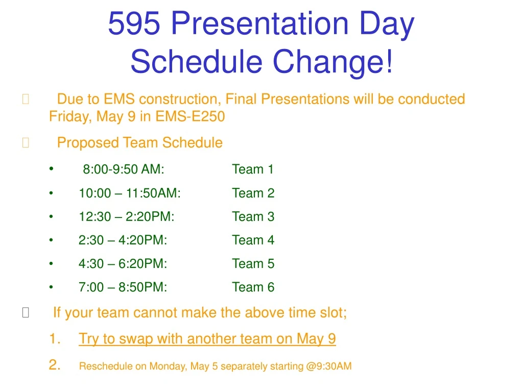
595 Presentation Day Schedule Change! • Due to EMS construction, Final Presentations will be conducted Friday, May 9 in EMS-E250 • Proposed Team Schedule • 8:00-9:50 AM: Team 1 • 10:00 – 11:50AM: Team 2 • 12:30 – 2:20PM: Team 3 • 2:30 – 4:20PM: Team 4 • 4:30 – 6:20PM: Team 5 • 7:00 – 8:50PM: Team 6 • If your team cannot make the above time slot; • Try to swap with another team on May 9 • Reschedule on Monday, May 5 separately starting @9:30AM
595 Presentation Day Schedule Change! • Lab sessions will be held at normal times Mon-Wed, May 5-7th • Monday, May 5 will be a Final Lab Session for LA-803 for prototype demonstration • Tuesday, May 6 will be a Final Lab Session for LA-802 for prototype demonstration • Wednesday, May 7 will be a Final Lab Session for LA-801 for prototype demonstration • Thursday, May 8th there will be NO lecture however teams may submit a preliminary presentation file for an optional ~20 min walk through in E225. (first come, first serve) • Project Reports (Printed & Electronic MSWord files) will now be due by 9PM in E250 on Friday, May 9
Presentation P3System Design Detailed Design • Objectives • Update Final Presentation with Block Detailed Designs Presentation P3 in Lab~60 Minute Time Limit Per TeamCome to Lab with 1 Consolidated File per Team Memory Stick or CD
Reuse/Update Presentation P1 • Team Deliverable • Reuse the following slides for P3 (leave out lined items) • All Project Proposals including block diagrams • Team Roster and Background Slides • Recommended Project Description • High Level or User Requirements – What does it do for user? • Perf Requirements Summary • Std Requirements Summary • Basic Business Case • Refined Block Diagram - Block Diagram Description Page • Requirements Spreadsheet: Project Level Tabs (Excel File) • Requirements Spreadsheet: Block Level Tab Flowdowns (Excel File) • 1 Page on 3 Key Patents Found for Product Area – Mitigation Plan • 1 Page on Key Ethical/Societal Risk Areas – Mitigation Plan Labs 1A-B Lab 1C
Reuse/Update Presentation P2 • Team Deliverable – Product Level Slides • Product Safety Mitigation Slides – Lab 2 • Product EMC Mitigation Slides – Lab 2 • Product Level Design Plan Summary & Gantt Chart Slides – Lab 3 • Overall Prototype Plan, Interconnection Strategy – Lab 3
Reuse/Update Presentation P2 • Individual Deliverable - Block Level Slides • Block Description and Purpose Slide • Block Performance Requirements, Allocated/Associated • Block Standard Requirements, Allocated/Associated • Block Signal Input/Output Summary Slide(s) – Lab 1C • Block Diagram Breakdown Slide (Block Diagram of the Block) • Block Preliminary Schematic - (Product Design !) • 3-4 Bullets on Theory of Operation • Block Preliminary Bill of Materials – (Product Design !) • Block Detailed Design Calculations & Component Selection – • See Next Page For Each Block ---- Required Slides Complete as much as possible to present in lab next week (prior to lab)
New Presentation P3 • Additional Product Level Slides – Lab 5 • Product Mfg Process Design (Block Diagrams) – Lab 5 • PCB Assembly Process Diagram including all Inspection & Testing • High Level Assembly Process Diagram including all Insp & Testing • Product Overall Master BOM – Lab 5 • Prototype Layout Exercise – Lab 5 Labs 2-3
Presentation P3 Additional Block Detailed Design Slide Content Detailed Design Calculations & Component Selections • Device Package Type Rationale • Nominal Resistance, Capacitance, Inductance Values & % Tolerance Calculations • Resistor Compositions, Capacitor Dielectric, Inductor Winding; Selection Rationale • Resistor, Capacitor, Inductor, Diode, Transistor & IC Max Voltage Calculations • Resistor, Inductor, Transistor, Diode, Xfmr, & IC Max Power Calculations • Power Electronics Heat Sink qj Calculations and Max Die Temp Rise Above Ambient • EMC Devices including filters, ferrites, transient absorbers, etc • Safety Devices such as Current Limiters incl Fuses, Breakers, GFCI, etc • Wire Gauges, Interconnect Contact, & Trace Width Ratings • Op-Amp Selections including Ib, Vio, CMRR, Slew Rate, Iout & Error Voltage Calculations • Logic Family Selection including Interface Compatibility, Speed, Power • CPU and/or PLD Types and Clock Speed, Performance Capabilities • Regulator Basic Performances incl % line and % load regulations • Nominal Time Domain Operational Simulations • Nominal Frequency Domain Operational Simulations • Worst Case or Monte-Carlo Simulations • Additional Analog Circuit DFM Analysis as applicable
All Components Require Some Level of DFM Justification • Passives: Resistors, Capacitors, Inductors, Thermistors • Semiconductors: Diodes, Transistors, SCRs, Triacs, Bridges, Integrated Circuits, etc • Sensors: Temp, Pressure, Humidity, Ph, Moisture, Distance, Proximity, etc • Transducers: Speakers, Microphones, Buzzers, Peizo, etc • Relays: Electro-Mech, Solid State, Reed, Latching • Motors: Drives, Solenoids, Linear Motors, Actuators • Transformers: Auto, Split, Center Tapped, Toroid, RF, Tuning • Batteries: Alkaline, NiCd, NiMH, LiIon, Pb Acid, etc • Interconnects: Wire, Connectors, Terminals, Power Plugs, Cables, Jacks, Plugs, etc • Switches: Toggle, Rocker, Momentary, Breakers, Keyboards, etc • Displays: Lamps, LEDs, Segmented Displays, LCDs, etc • Over Current Protection Devices: Fuses, Breakers, GFCI, Surge Protectors • Over Voltage Protection Devices: Diodes, Fast Clamps, Tranzorbs • Other Safety & EMC Devices: Ferrite Beads, Chokes, Line Filters, Shielding Why was this particular manufacturer’s part number picked? What are the most important part attributes and how have you guaranteed DFM?
Common Analog & Power Subcircuits for DFM Analysis Non-Linear Linear • Comparators • Oscillators (non-sinusoidal, square, sawtooth, etc) • Voltage Limiters and Clamps • Rectifiers and Bridges • Math Functions (multiply, divide) • Log and other Non-linear Amplifiers • Sample and Hold Amplifiers • Envelope & Peak Detectors • Phase Detectors • Phased Locked Loops • Switching Voltage Regulators • Pulse Generators, Debouncers • Multipliers, Modulators, Transmitters, Receivers • Amplifiers and Attenuators • Math Functions (add, subtract) • Oscillators (sinusoidal) • Filters • Voltage Regulators • Voltage References • Analog Drive Displays (Bulbs, LEDs, etc)
Common Digital Subcircuits for DFM Analysis Logic Family Based LSI & VLSI • Adders, Subtractors, Math Units • Magnitude Comparators • Encoders • Decoders • Multiplexers (Mux’s) • Demultiplexers (Dmux’s) • Code Converters • Bus Buffers • Flipflops, Latches, Latching Buffers • Counters, Timers • Pulse Generators • Optical Couplers • CPU’s & Microcontrollers • Analog-Digital Converters • Digital-Analog Converters • Prog Logic Devices, FPGAs • Sequencers • Prog Read Only Memories (Eproms, EEproms) • Random Access Memories (SRAM, DRAM) • Controllers (Serial, Drive, USB, Ethernet) • Logic Input Displays