Download
1 / 35
350 likes | 525 Vues
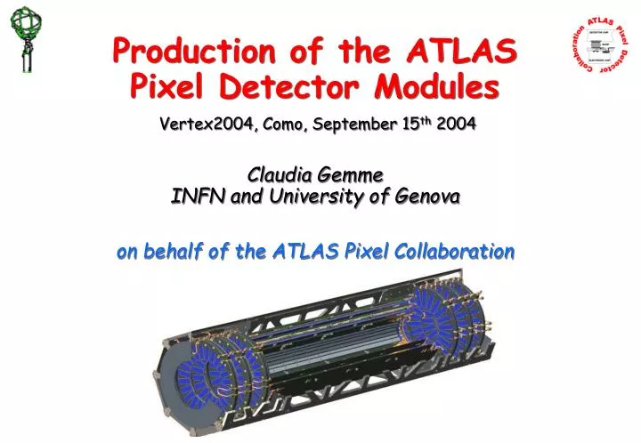
Production of the ATLAS Pixel Detector Modules Vertex2004, Como, September 15 th 2004 Claudia Gemme INFN and University of Genova on behalf of the ATLAS Pixel Collaboration. ~380 mm. ~1850 mm. The ATLAS Pixel Detector. It is the innermost part of the silicon vertex tracker .

E N D
Production of the ATLAS Pixel Detector Modules Vertex2004, Como, September 15th 2004 Claudia Gemme INFN and University of Genova on behalf of the ATLAS Pixel Collaboration
~380 mm ~1850 mm The ATLAS Pixel Detector • It is the innermost part of the silicon vertex tracker . • It consists of two parts: • Barrel: 3 layers (12 cm, 10 cm and 5 cm radii); • End-cap: 3+3 forward-backward disks. • Only the ‘reduced’ layout is approved (2 layers +2+2 disks), due to budget reason: the 3-layer system may be approved soon. • Going from 3 to 2-layer system means a reduction of 30%. • ~1.7 m2 of sensitive area with 67M (barrel) + 13M (disks) channels. • Total dose 50 Mrad on the middle layer in 10 years of LHC. • Installation foreseen mid-2006
Flex Hybrid MCC sensor FE chip FE chip Pixel Modules • Modules are the basic building elements of the detector (1456 in the barrel, 288 in the end-caps). • Each module has an active area of 16.4 mm x 60.8 mm. • The sensitive area is read out by 16 FE chips which are controlled by a Module Controller Chip (MCC). Each FE read-outs 2880 channels organized in a matrix of 18x160 channels. Each pixel has a 400mm x 50mm area. • A Flex-Hybrid circuit glued on the sensor backside provides the signal/power routing. the signal routing between the 16 FE chips and the MCC. • A pigtail (only for barrel modules) + Al/Cu wire bundle connect flex hybrid to patch panels at either end of pixel detector. Pigtail is the only difference between barrel and disks modules. Wirebondings Schematic cross section (through here) bumps
Work packages (PPT) da sostitire con una frase o schema piu’ semplice ( e in inglese) Fornitura di chip da LBL Target 20/sett. Target >10/sett.
Production Status of basic components: Sensors Electronics Flex Hybrids
Sensors (necessary? Ci passi veloce…5”) • Baseline design: • n+ pixel in n-bulk material: • Moderated p-spray isolation. • Bias grid to allow testing before module assembly. • Oxygenated silicon to improve radiation resistance and increase allowable time to room temperature (for repair/upgrades). • Two vendors: Cis and Tesla 3 tiles wafer, n side Charge collection efficiency (meas) n+ implants and bias grid
Sensors Production • Two vendors have produced the sensor tiles: • CiSdelivered1121good tiles during 2002/03. All of them have been tested and 1094 are fine. A replacement of 55 tiles is on-going. • Tesla (nowON Semiconductor) began its deliveries in April 04. After an initial yield problem, now it is ending its 900 tiles contract. The only problem for us is the lower fraction of wafers with 3 good tiles (24% ON). Rifare il totale?
Sensors Production • Performances are very similar between ON and CIS. • We have the possibility (option expiring Feb05) to order other tiles if the 3-layers project will be definitevely approved. • Testing is done in 4 labs and 100 tiles/months could be easily achieved thus ending the test of the delivered tiles in ~6 months time.
Optical Driver (VDC) FE chip MCC 100m sensor FE chip 1m Optical Receiver (DORIC) ….. power optical LVDS control HV bias bump bonds LVDS data out On-detector Electronics • On-detector chips are fabricated in 0.25mm DSM by IBM. Used circuit library with special layout rules for radiation tolerance. • MCC: decode data/cmd signals, generate control signal for 16 FEs, collect data from FEs and accumulate in FIFOs, check event consistency, build module event and sends to DAQ, handle errors. • FE chip: control 18x160 pixels. Amplify sensor signal, on-chip data buffering in EOC FIFOs until trigger signal arrives, send data on serial link to MCC.
3 1 4 2 6 5 8 7 MCC-I2.1 • After one year of experience with modules of first generation DSM, we have received back in May03 the second generation of chips (MCCI2). • Some problems have been easily fixed and respin of wafers not completely processed has produced chips good for production (MCCI2.1) . • Out of 6 wafers we have obtained 2666 good MCC-I2 with a yield of 83% (1744 needed in the 3-layers detector).
FEI3: Wafer status • The first engeneering run (6 wafers) was delivered in Dic 03. • After that, we received three production runs (48 wafers each). Another two are expected in the next months, before the end of the year. • A complete test on each chip is performed at the wafer level (LBL and Bonn).Testing speed is coping well with deliveries. • The mean yield on wafer is 79% (but varies from 60 to 92%,sembra migliorare ultimamente )
FEI3: Good dies status • An electric test and a visual inspection are performed after wafer bumping deposition, thinning and dicing on the singled dies. • Yield of electric test is very high: 99.4% (however on modules would mean 90% yield); • Yield of visual inspection is 88% (mainly damaged bumps); this step is critical as debris can damage the chip or the sensor after flip-chipping. • Considering a yield of 79% at wafer level and ~ 85% at chip level, having 288 chips on each wafer, we get 11-12 modules/wafer. • IBM will deliverd a total of 246 wafers thus sufficient for more than 2700 modules,i.e enough for the 3-layers detector.
Flex Hybrid • 2000 delivered and tested. • 1000 more delivery foreseen Oct 1st. • SMD are mounted on the kapton, then the Flex is glued on a frame that will be used for further tests. This frame makes easy the module handling until it is cut to be loaded on its final support.
Module Assembly and Testing (da animare) Flex+MCCGenova/Bonn/LBL PigtailBonn 16 FEs Sensor ON/Cis Bare moduleAMS/IZM MCC operation + connectivity Elco connectivity Bare module test 2 1 Flex+MCC+Pigtailgluing PT wire bonding HV+voltage drop+peel test Flex modulegluing wire bonding/ pull potting Post burn-in test Burn-in Assembly test 3 Sorting for loading Cold full characterization 4
16 thinned FEs, ~50k bumps 16.4mm Sensor AMS - In IZM – PbSn 60.8mm Bare Modules (si deve capire che e’ lo step 1) • Hybridization is done by AMS and IZM. It consists of bump deposition on wafer, thinning and cutting FE-wafers (in US), cutting of sensor tiles and flip-chip of 1 tile with 16 FEs. • Techniques are different but electrical results and yield are comparable. • Tests on the bare module before further assembling are: • A X-rays scan to verify the quality of bumps; • A visual inspection and IV curve; • An electricaltest contacting each chip individually. In case of failure, a chip reworking can be tried (i.e. chip substitution). • Total test time: 2h/module.
QA check using X-rays • Yield on x-ray is very high. • Few chips (HOW?) not attached and one rotated in AMS.
Yield bare modules Yield is (90+21)/134=83% and (71+10)/87=93% (IZM) Losses in reworking is 7/28 (AMS) and 2/12 (IZM) (There are a few accepted re-worked bare modules that failed later. some bare module rejection after rework will be needed. Should be order 2%) Main problems in the table Rifare I grafici piu’ chiari Eventualmente Aggiungere la frazione di AVDD Rispetto alle failure totali Come nella slide 32
Fragment on the electronic chip (reworking possible) or on the sensor (reworking not possible). DVDD/AVDD shorts • VDDA/DVDD shorts represents the first cause of failure (80%??). • VDDA/DVDD shorts show up as about 300 mA current at power up (instead of few mA) on the analog (mainly) or digital supply. • They are due to silicon fragments which get trapped between the bumps and damage the electronics when pressure is applied during the flip-chipping. • These fragments are due to back-side chipping during dicing. • These particles are hard to be recognized during the visual inspection and moreover they could reach the bumps even during the shipments/handling. • Some attempts to reduce the problem have been tested (changing dicing parameters and/or polishing wafers, improving cleaning before flip-chipping), but for the time being we should live with this problem (i.e. rework).
Flex Hybrid Assembling (si deve capire che e’ lo step 2) • Critical point is the MCC bonding as, due to the geometrical limitations, the bonding loop can not be standard. • Using an Al 25um wire we get a large fraction of peel off or lift (63%)even if obtained with a sufficiently high mean force (12g). • Alternative solutions are under study: • 2 bondings, 17 um each per pad; • Gold ball bonding (not much experience) • …
Module Assembling (si deve capire che e’ lo step 3) • Assembling modules is a complex operation but we have a large experience so that in each lab 10-15 modules can be assembled per week (expected rate from bump-bonding firm is 30 modules/week). • For each module a pull- test is done: 20 bondings are pulled in order to qualify the quality. We still have some not-stick bondings when cleaning is not perfect. Inserire un plot con DGRID force
Potting • Potting e’ fatto sui bonding del pigtail, MCC, HV e dei FE. • Reworking di questo potting e’ possibile. • Aggiungere test di risonanaza e perche’ abbiamo deciso di pottare solo I piedi (vedi articolo Amanda)
Test Flex Modules (si deve capire che e’ lo step 4) • Up to now module testing is the longest operation: even if all the tests are completely automatized, ~10 modules/week/lab is the maximum speed (this means ~40-50 modules/week in the collaboration).
FEI3 modules yield • Yield of Flex module assembling/burn-in and testing is ~95%.
Module problems • Problems mainly showed up in the very first electrical tests. • No infant mortality has been observed so far after/during the burn-in. • We have observed few modules in which the AVDD/DVDD shorts appeared after few hours of electrical functioning. • The main problems are (see table): AVDD/DVDD shorts not observed at the bare module level, MCC faults, Elco connector faults. • Some of these problems will be reduced as we have had more tests on the components before module assembling; other are intrinsic and will not decrease.
Merged bumps (questo forse e’ un po’ troppo specifico…) • Sometimes merged bumps have been observed on the edge columns of AMS modules. • This kind of defect have been traced to an excessive depth of the shim in some Genova test boards. Add a small picture with a threshold scan for a channel to explain what the plot is.
Source scan (questa e la seguente si possono evitare) • Source SCAN with source located on the module centre (distance source-module ~ 3cm, source: 241Am, 10 mCi). • If the source stays on the module centre, the scan takes 4hours/200kevs. • If the source is moved on the scanned chip, it takes 2-3 min/200Kevs.
Fe 9 Fe 8 Fe 6 Fe 7
PDB & raw data server (Necessary?) • Penso sia necessario dire che e’ necessario e che lo abbiamo, niente di piu’.
Conclusions • Module Production has started: components are there and assembling and testing are fine. • We still have some critical step that we are better investigating (MCC wire-bonding, dealing with dies back-side chipping to reduce reworking). • Data analysis for sorting is to be finalized soon. • Emphasis is now moving on the next steps: loading on local supports! Sector front side: 3+3 modules Stave: 13 modules
Yields • AMS chip probing: • Electrical: 99.4 +/- 0.1%, Visual: 86% • Bare Modules