Download
1 / 22
810 likes | 1.64k Vues
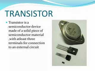
TRANSISTOR. TRANSISTOR Background and Introduction. A semiconductor device that Amplifies, Oscillates, or Switches the flow of current between two terminals Invention of the Transistor

E N D
TRANSISTORBackground and Introduction • A semiconductor device that Amplifies, Oscillates, or Switches the flow of current between two terminals Invention of the Transistor American physicists John Bardeen, Walter H. Brattain, and William Shockley(later jointly awarded a Nobel Prize) It was also independently developed nearly simultaneously by Herbert Mataré and Heinrich Welker, German physicists working at Westinghouse Laboratory in Paris. First Transistor Model, 1947
Transistor Material • The transistor is an arrangement of semiconductor materials that share common physical boundaries. • Materials most commonly used are • Silicon • gallium-arsenide • and germanium • Impurities have been introduced by a process called “doping”
TYPES OF TRANSISTOR • BJT • Bi Polar Junction transistor • FET • Field effect transistor
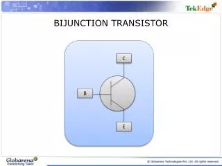
BJT • A BJT (Bipolar Junction Transistor) transistor has inside two similar semi conductive materials, and between them there is a third semi conductive material of different type • if the two similar materials are P and the middle one is N, then we have a P-N-P or PNP transistor. • if the two materials are N and the middle one is P, then we have a N-P-N material or NPN • Each transistor has 3 leads which we call base, collector and emitter, and we use the symbols b, c and e respectively • The symbol of the transistor has an arrow on the emitter. • If the transistor is a PNP, then the arrow points to the base of the transistor, otherwise it points to the output.
Types Of BJT • Two basic types of bipolar junction transistor construction, • PNP • NPN, • which basically describes the physical arrangement of the P-type and N-type semiconductor materials • n-type semiconductorsthe impurities result in an excess of electrons, or negative charges • p-type semiconductorsthe material lead to a deficiency of electrons and therefore an excess of positive charge carriers or “holes.” • current regulating devices that control the amount of current flowing through them
BJT Basic construction The BJT is a three terminal device that produce two PN junctions • Emitter ( E ) • Base ( B ) • Collector ( C ) Principle of operation of the two transistor types PNP and NPN • Biasing • polarity of the power supply for each type Collector Base Emitter
EMITTER • It is highly doped • To inject a large number of charge carriers • Main function is to supply the majority carriers to the base. • It is always forward biased with respect to base
BASE • It is a middle section of a transistor • It is lightly doped • So that most of the charge carriers pass to the collector. • It controls flow of charges • It forms two PN junctions with Emitter and Collector
COLLECTOR • IT IS situated opposite to the emitter • It is always reversed biased • So that it can collect the majority carriers • Size of collector is larger than emitter • Its doping level is in the middle of base and emitter
NPN TRANSISTOR • It is constructed by two N type and One P type material. • Emitter and collector are of N type material • Base is of P type material • It consist of two PN junctions Sandwiching a P-type layer between two n-type layers.
OPERATION OF NPN TRANSISTOR • The base-emitter diode is forward biased • The base-collector diode is reverse biased • VBE injects the electron to the Emitter. • Emitter is highly doped • Base is lightly doped • Collector creates electrostatic field which • Attracts the electrons • 95 to 99% electrons diffuses in • collector region E C B backward Forward VCB VBE
Transistor operation With no power applied to the transistor areas • There are two depletion zones between the two P-N contacts. Power source Connected b/w base and collector in reverse-bias • With the positive of the source connected to the collector and the negative to the base. • The depletion zone of the P-N contact between the base and the collector will be widened. • A slight current will flow within this contact (due to impurities). • This current is the reverse contact current symbol ICBO
Transistor operation Voltage supply between the emitter and the base in forward bias • With the positive of the source connected to the base and the negative connected to the emitter. • The depletion zone between the emitter and the base will be shortened • current (electrons) will flow when the voltage exceeds a specific level. • This level depends on the material that the transistor is made of. • Some of the electrons that go through the e-b depletion zone, will re-connect with holes in the base. • This is the base current IB symbol for reference. • In real life, this current is at the scale of micro-amperes (μA ):
Cont’d • Most of the electrons will flow through the base (due to spilling) and will be directed to the collector. • When these electrons reach the depletion area between the base and the collector, they will experience a force from the electric field which exists in this zone, • The electrons will pass through the depletion zone. • The electrons will then re-connect with holes in the collector. • The re-connected holes will be replaced with holes coming from the base-collector power supply (VCC). • The movement of these holes equals to a movement of electrons in the opposite direction, from the collector to the supply. • In other words, the current that flows to the emitter will be divided into the small base current and the larger collector current: IE = IB + IC
Cont’d • Generally, the number of electrons that arrive at the collector is the 99% of the total electrons, and the rest 1% causes the base current. • At the collector, except the electrons that come from the emitter, there is also the reverse current from the base-collector contact • Both currents flow at the same direction, so they are added IC' = IC + ICBO
Transistor Parameters and Ratings • The ratio of the dc collector current (IC) to the dc base current (IB) is the dc beta (bDC). • bDC is called the gainof a transistor: • bDC = IC/IB • Typical values of bDC range from less than 20 to 200 or higher. • bDC is usually designated as an equivalent hybrid (h) parameter: • hFE = bDC • The ratio of the collector current (IC) to the dc emitter current (IE) is the dc alpha (aDC). This is a less-used parameter than beta. • aDC = IC/IE • Typical values range from 0.95 to 0.99 or greater. • aDC is always less than 1. • This is because IC is always slightly less than IE by the amount of IB.
Cont’d There are a number of standard parameters that are used to define the performance of a transistor. Some of them are given below • Type number • Case • Material • Polarity • VCEO Collector emitter voltage with base open circuit • VCBO Collector base voltage with the emitter open circuit • VEBO Emitter base voltage with collector open circuit I • C Collector current • ICM Peak collector current • IBM Peak base current • PTOT Total power dissipation • Tamb Ambient temperature T
Cont’d • Stg Storage temperature. • ICBO Collector base cut-off current • IEBO Emitter base cut-off current • hFE Forward current gain • VCEsat Collector emitter saturation voltage • VBEsat Base emitter saturation voltage • Cc Collector capacitance • Ce Emitter capacitance • Ft Frequency Transition
Introduction to Amplifiers • The BJT is an excellent amplifier when biased in the forward-active region. • The FET can be used as an amplifier if operated in the saturation region. • In these regions, the transistors can provide high voltage, current and power gains. • DC bias is provided to stabilize the operating point in the desired operation region. • The DC Q-point also determines • The small-signal parameters of the transistor • The voltage gain, input resistance, and output resistance • The maximum input and output signal amplitudes • The overall power consumption of the amplifier