Download
1 / 4
40 likes | 142 Vues
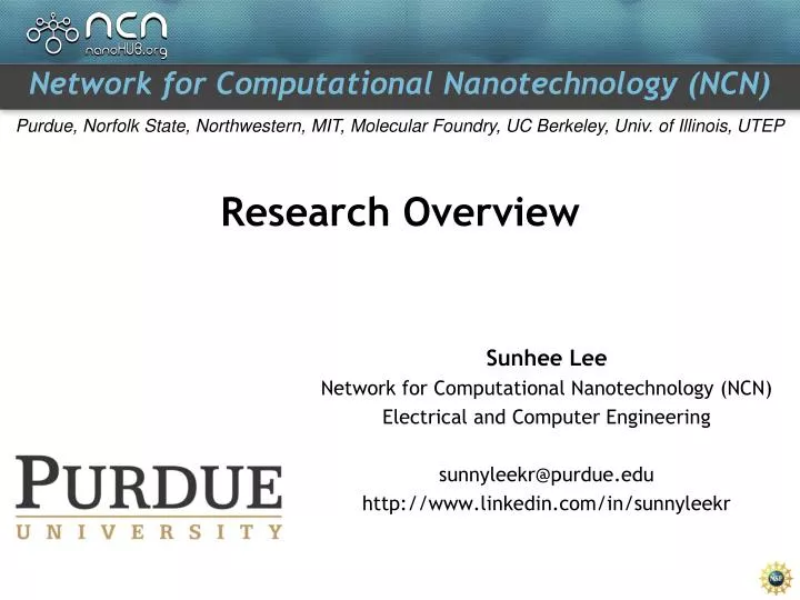
Research Overview. Sunhee Lee Network for Computational Nanotechnology (NCN) Electrical and Computer Engineering sunnyleekr@purdue.edu http://www.linkedin.com/in/sunnyleekr. Network for Computational Nanotechnology. Nanotechnology Atomic scale (10 0 ~10 2 nm)

E N D
Research Overview Sunhee Lee Network for Computational Nanotechnology (NCN) Electrical and Computer Engineering sunnyleekr@purdue.edu http://www.linkedin.com/in/sunnyleekr
Network for Computational Nanotechnology • Nanotechnology • Atomic scale (100~102 nm) • Old device physics breaks down • New device, materials, geometry, fabrication methods or concepts • Computation • Simulations • Theory (bottom-up approach) • Tool development (nanoHUB.org) BJT Lab @ nanoHUB Yui, Nano Lett. 09 Graphene 30nm HEMT from MIT M.Fueschle, Nature 09 Quantum Dot Quantum Dot Lab @ nanoHUB http://nanohub.org Chin et al. IEDM 09 Si Nanowire Professor S. Datta • Network • Experimentalists • Research and publications • Education
R&D Overview • Research • Electronic properties of densely doped planar silicon devices • Tool development • Develop a quantum mechanics based 3-D NanoElectronic MOdeling tool (NEMO 3-D) • Features • Atomistic description of device • Self-consistent calculation • Efficient parallel computation • Engine for nanoHUB tool(s) Densely doped P atoms on silicon New Fabrication steps • Approach/Results • Atomistic tight-binding calculation • Self-consistent method
Qualifications and Plans • Plan A: Academia/Research institute • Computational science • High-performance computing • Numerical engineering • Plan B: Back to industry • Device design / design tool development • Semiconductor companies • Intel / Samsung • Academic experience • Device physics background • Co-author of 20+ publications • Software skills • C/C++/Java/HTML/Linux • Cluster computing • Industry experience • Software engineer (5.5yrs) • Developed software for network terminals (cable modems, voice over IP terminals, set-top boxes) • Knowledge of network and communication • Mass production know-how • Embedded programming