Download
1 / 32
320 likes | 331 Vues
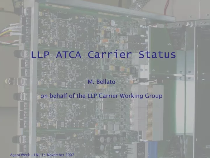
LLP ATCA Carrier Status. M. Bellato on behalf of the LLP Carrier Working Group. Agata Front-end Model. Clock Distribution. From GTS Tree. (***) User SFP could be used as 1GEnet or PCIExpress DAQ without FABRIC. MGT clocking layout. MGT Clocking Layout. RocketIO 101.

E N D
LLP ATCA Carrier Status M. Bellato on behalf of the LLP Carrier Working Group
Clock Distribution From GTS Tree
(***) User SFP could be used as 1GEnet or PCIExpress DAQ without FABRIC MGT clocking layout MGT Clocking Layout RocketIO 101 RTM PCI EXPRESS LANE1 A B MUX RTM PCI EXPRESS LANE0 MGTclk M34/N34 RocketIO 102 200MHz GTS Clock USER SFP TRANSCEIVER MUX A B MGTclk AP28/AP29 RocketIO 103 ATCA FABRIC CH11-CH12 MUX A B PHASE LOCKED RocketIO 105 100MHz GTS Clock A B MUX ATCA FABRIC CH9-CH10 INSPECTION PADS RocketIO 106 LOCAL 100MHz (EPSON) A B ATCA FABRIC CH7-CH8 MUX RocketIO 109 ATCA FABRIC CH5-CH6 A B MUX MGTclk AP3/AP4 RocketIO 110 ATCA FABRIC CH1-CH2 A B MUX 100250MHz PCI Express JITTER ATTENUATOR MGTclk J1/K1 RocketIO 112 A B MUX ATCA FABRIC CH3-CH4 RTM PCI EXPRESS LANE5 RocketIO 113 INSPECTION PADS A B RTM PCI EXPRESS LANE4 MUX (**) The ATCA FABRIC channels are routed from CHANNEL1 to CHANNEL12 by switches RocketIO 114 RTM PCI EXPRESS LANE3 OPTICAL SFP A B MUX RTM PCI EXPRESS LANE2
Carrier Power Supply 4x LTM4600 55W DC to DC Converter P3V3-5A 16.5W P3V3/P2V5 Linear Reg P2V5-1.5A VCCAUX Fpga 1 MEZZANINE 1 DC to DC Converter Fusing Filtering Protection Hot Swap P3V3-5A 16.5W MEZZANINE 2 P5V0/P2V5 Linear Reg P2V5-1.5A VCCAUX Fpga 2 -48V DC DC to DC Converter P5V0/P2V5 Linear Reg P2V5-1.5A P3V3-5A 16.5W MEZZANINE 3 VCCAUX MGT DC to DC Converter P5V0/P1V8 Linear Reg P1V8-0.5A P3V3-5A 16.5W MEZZANINE 4 PROMS ENABLE P5V0/P1V2 Linear Reg P1V2-0.5A ATC210 (210W) VTTTXs P12V-14.7A 176.7(160.6)W M48/P12 DC DC P5V0-6A 30W P5V0/P1V2 Linear Reg P1V2-0.5A VTTRXs P12/P5V0 DC DC M48V-4.0A 194.4(176.7)W P3V3_BOOT P3V3-7A 23.1W P12/P3V3 DC DC MAIN BOARD P12/P2V5 DC DC P2V5-7A 17.5W MAIN BOARD P12/P1V2 DC DC P1V2-7A 8.4W FPGAs CORE DC-DC Efficency is estimated at least 90% P12/P1V2 DC DC P1V2-4A 4.8W FPGA MGT P12/P1V8 DC DC P1V8-6A 10.8W MGT BUFFERS 6x LTM460055W
Carrier main features 1M x 18 true dual port RAM @ 100/200 MHZ 800Mb/s LVDS streaming on data channels Equalized and filtered distribution of 200MHZ GTS clock 1 PCI Express/ GE optical link 15 x Full mesh connectivity on the backplane Pervasive I2C bus for slow controls 200W power supply Multiple options for data readout
Tests Campaign • Started in august • still going on • >18 different tests • Jtag chains • FPGAs configurations • Power distribution • I2C control chains • 200 MHz Clock distribution • Microprocessor • Sdrammems • Flash mem • Dual port ram • PLL • PCI Express optical link • Fast Ethernet switch + PHY’s • MII connections • Backplane 2.5 Gb/s serial links • Mezzanine connections • 800 Mb/s LVDS lanes • Trigger distribution • Master/slave functionality
1 0 1 0 1 0 1 0 1 0 1 0 1 1 1 0 0 0 1 1 1 0 0 0 Serdes Advantage ChipSync™ FPGA Fabric ISERDES 0 1 1 0 0 CLK CLKDIV Clk Div BUFIO BUFR Data width of of 2, 3, 4, 5, 6, 7, 8, 10
Bit Alignment ChipSync™ CLK FPGA Fabric ISERDES IDELAY DATA INC/DEC State Machine 190-210 MHz(calibration clk) IDELAY CNTRL • 64 delay elements of ~ 70 to 89 ps each • Calibration clock can be internal or external
INC DEC State Machine Clock Sampling Phase Adjust
Word Alignment ChipSync CLK ISERDES FPGA Fabric DATA State Machine BITSLIP Up to 10-bit bitslip pattern for any length training patterns
DATA1 1 1 0 0 0 1 0 0 0 0 0 1 0 0 0 1 0 0 0 0 1 1 0 1 0 1 0 0 1 1 1 1 1 1 1 0 1 0 1 1 0 0 0 0 0 0 0 1 0 1 0 1 1 0 1 1 1 1 0 1 1 0 1 DATA2 DATA3 Bitslip 3 Bitslip 2 Bitslip 1 Word Alignment Animation State Machine
Spice Verification • S-parameters of a lvds pair from Mictorconns to main FPGA through full wave EM solver • Encrypted Hspice model of lvds25ext pad from Xilinx • Hspice simulation
PCI Express Readout Test Int *ATCA0 = 0xfe001000; // DPRAM on board 0 Int *ATCA1 = 0xfe002000; // DPRAM on board 1 …. Fragment0 = memcpy(buffer0, ATCA0); Fragment1= memcpy(buffer1, ATCA1);
Status Tests ongoing • Excessive noise on DC/DC converters - not suitable for high speed operation • Central reset manager missing • Some errors on components footprints • 90% completed Modifications already ongoing at CERN • The layout will be frozen until the end of tests Procurement of components for 2 pre-production boards ongoing
Schedule Expected layout completion : end of Dec 07 Signal integrity analysis end of Jan 08 2 x PCB manufacturing : Feb 08 2 x PCB assembly : Mar 08 2 x Board tests Apr 08