Download
1 / 25
250 likes | 382 Vues
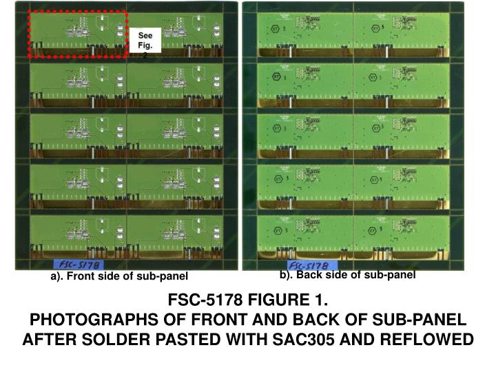
b). Back side of sub-panel. a). Front side of sub-panel. FSC-5178 FIGURE 1. PHOTOGRAPHS OF FRONT AND BACK OF SUB-PANEL AFTER SOLDER PASTED WITH SAC305 AND REFLOWED.

E N D
b). Back side of sub-panel a). Front side of sub-panel FSC-5178 FIGURE 1. PHOTOGRAPHS OF FRONT AND BACK OF SUB-PANEL AFTER SOLDER PASTED WITH SAC305 AND REFLOWED
FSC-5178 FIGURE 2. MAGNIFIED VIEW OF FRONT SIDE OF TI +5V GATE DRIVE DISCRETE DUT CARD 10030 Rev 2-T AFTER SOLDER PASTED WITH SAC305 AND REFLOWED
See Fig. 22 C D B A FSC-5178 FIGURE 3. MAGNIFIED VIEW OF Q1, Q2, AND Q3 FOOTPRINTS WITH ‘PURPLE” DISCOLORATION
FSC-5178 FIGURE 4. MAGNIFIED VIEW OF OTHER FEATURES ON CARD THAT DON’T HAVE “PURPLE” DISCOLORATION
FSC-5178 FIGURE 5. MAGNIFIED VIEW OF OTHER GOLD PLATED EDGE FINGERS
PCB Surface Finish is Electrolytic Gold / Nickel FSC-5178 FIGURE 6. XRF SPECTRUM OF PLATED EDGE FINGERS
X X X X X X X X X X X X X X X X X X X X X X X X X X X X X X X X X X X X X X X X X X X X X X X X X X FSC-5178 FIGURE 7. 3D SURFACE PLOT OF XRF MEASUREMENT OF ELECTROLYTIC GOLD (Au) PLATING THICKNESS
X X X X X X X X X X X X X X X X X X X X X X X X X X X X X X X X X X X X X X X X X X X X X X X X X X FSC-5178 FIGURE 8. 3D SURFACE PLOT OF XRF MEASUREMENT OF ELECTROLYTIC GOLD (Au) PLATING THICKNESS
FSC-5178 FIGURE 9. FREQUENCY DISTRIBUTION OF XRF MEASUREMENT OF ELECTROLYTIC GOLD ON EDGE FINGER
FSC-5178 FIGURE 10. FREQUENCY DISTRIBUTION OF XRF MEASUREMENT OF ELECTROLYTIC GOLD ON EDGE FINGER
FSC-5178 FIGURE 11. FREQUENCY DISTRIBUTION OF XRF GOLD MEASUREMENT ON BACK SIDE DISCRETE COMPONENT PADS
FSC-5178 FIGURE 12. FREQUENCY DISTRIBUTION OF XRF NICKEL MEASUREMENT ON BACK SIDE DISCRETE COMPONENT PADS
PCB Solder Consistent with SAC305 FSC-5178 FIGURE 13. XRF SPECTRUM OF SOLDER ON Q3 FOOTPRINT
Corner of Q3 footprint is Electrolytic Nickel/Gold FSC-5178 FIGURE 14. XRF SPECTRUM OF NON-WET PORTION OF Q3 FOOTPRINT
Leading edge “wave” is consistent with SAC305 that has lots of Au dissolved in it FSC-5178 FIGURE 15. XRF SPECTRUM OF LEADING EDGE ‘WAVE” AT CORNER OF Q3 FOOTPRINT
FSC-5178 FIGURE 16. XRF SPECTRUM OF “PURPLE” AREA ON Q3 FOOTPRINT
a). Upper left corner of Q3 pad b). Upper left corner of Q3 pad after cleaning with dilute (~3%) muriatic acid FSC-5178 FIGURE 17. PURPLE DISCOLORATION IS EASILY REMOVED WITH DILUTE MURIATIC ACID
Purple area appears to be loaded with Intermetallic needles Area Dispensed with SAC305 Solder Paste FSC-5178 FIGURE 18. MAGNIFIED VIEW OF PURPLE AREA AFTER REMOVAL WITH DILUTE MURIATIC ACID
See Fig. 20 FSC-5178 FIGURE 19. CROSS SECTION OF Q2 FEATURE ON TI DUT CARD
a). Q2 cross section (25x) b). Q2 cross section (500x) SAC305 Solder Electroless Nickel (ENi) Copper Feature SAC305 Solder Sn-Ni IMC ENi c). Q2 cross section (1000x) FSC-5178 FIGURE 20. MAGNIFIED VIEWS OF Q2 FEATURE CROSS SECTION
a). 45° view of Q2 cross section (10x) b). Q2 cross section (50x) No Purple SAC305 Solder Purple SAC305 Solder Purple ENi ENi ENi c). Q2 (500x) Plated Cu Plated Cu d). Q2 (500x) Plated Cu e). Q2 (500x) Vendor Cu Vendor Cu Vendor Cu FSC-5178 FIGURE 21. MAGNIFIED VIEWS OF Q2 FEATURE CROSS SECTION SLIGHTLY FURTHER INTO Q2
Corner of Q3 cut to fit in SEM B C D A FSC-5178 FIGURE 22. FEATURE Q3 EXCISED FOR SEM/EDS ANALYSIS
A B See Fig. 24 A B D C D C b). Optical Image a). SEM Image FSC-5178 FIGURE 23. SEM AND OPTICAL IMAGE OF Q3 SAMPLE USED FOR SEM/EDS ANALYSIS
A B D C FSC-5178 FIGURE 24. MAGNIFIED SEM IMAGE OF Q3 SAMPLE USED FOR SEM/EDS ANALYSIS
SEM/EDS Analysis Comments • SEM/EDS isn’t a good technique to analyze thin discoloration on surfaces but it is the only analytical tool we have. • We used a low kV (10kV) to minimize penetration depth • The high Au (90.3%) on area ‘C’ indicates ENIG not wet with solder which agrees with optical yellow color. • The high Au (11.5%) on area ‘D’ indicates that the leading edge of the solder wave that is flowing out from where the solder paste was deposited dissolves Au from the ENIG as it wets and flows outward making the Au concentration higher at the leading edge. • The slightly higher O at the purple colored area ‘B’ (2.0%) and purple colored area ‘D’ (1.7%) may indicate that the purple discoloration may be a very thin oxide. • The high Sn at area ‘A’ (79.7%) and area ‘B’ (86.2%) and area ‘D’ (78.3%) as well as Ag at area ‘A’ (3.3%) and area ‘B’ ( 1.7%) and area ‘D’ (1.9%) indicate there is certainly SAC solder on those surfaces. • Auger or XPS would be a better surface analysis technique but we don’t have them.