Download
1 / 48
480 likes | 722 Vues
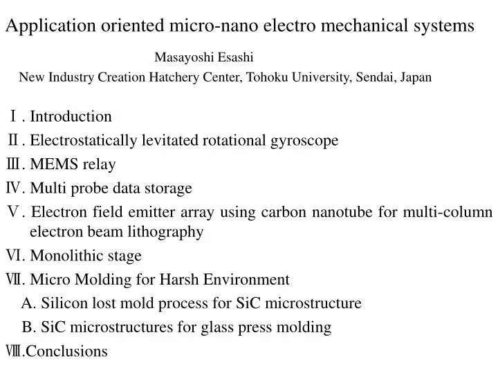
Application oriented micro-nano electro mechanical systems Masayoshi Esashi New Industry Creation Hatchery Center , Tohoku University, Sendai , Japan Ⅰ. Introduction Ⅱ. Electrostatically levitated rotational gyroscope Ⅲ. MEMS relay Ⅳ. Multi probe data storage

E N D
Application oriented micro-nano electro mechanical systems Masayoshi Esashi New Industry Creation Hatchery Center, Tohoku University, Sendai, Japan Ⅰ. Introduction Ⅱ. Electrostatically levitated rotational gyroscope Ⅲ. MEMS relay Ⅳ. Multi probe data storage Ⅴ. Electron field emitter array using carbon nanotube for multi-column electron beam lithography Ⅵ. Monolithic stage Ⅶ. Micro Molding for Harsh Environment A. Silicon lost mold process for SiC microstructure B. SiC microstructures for glass press molding Ⅷ.Conclusions
Vibrating gyroscope (yaw rate sensor) for vehicle stability control
Resonating gyroscope fabricated using Si deep RIE Si deep RIE system (M.Takinami, 11th Sensor Symposium, (1992) p.15)
Electrostatically levitating micromotor for rotational gyroscope (disk rotor type) (T.Murakoshi (Tokimec Inc.) et.al., Transducers’99)
Electrostatically levitating micromotor for rotational gyroscope (disk rotor type) (T.Murakoshi (Tokimec Inc.) et.al., Transducers’99)
10mm Electrostatically levitating micromotor for rotating gyroscope
Max 20,000 rpm 5mm
Rotor position is capacitively detected and voltage is applied to electrode (T.Matsubara et.al., Transducers’93, 50-53)
Electrostatically levitating micromotor for rotational gyroscope (ring rotor type) (Control voltage < 15 V) (T.Murakoshi et.al. : Jpn. J. Appli. Phys., 42, Part1 No.4B (2003) pp.2468-2472)
Structure of electrostatically levitated ring rotor gyroscope
Fabrication process of electrostatically levitating micromotor for rotational gyroscope (ring rotor type) Gap 5μm (100μm deep) Lateral control electrode Rotor
Rotor Noise floor Gyro : 0.002 deg/s/√Hz Accelerometer :10μG/ √Hz Inertia measurement system for 2-axis rotation and 3-axis acceleration MESAG-1 (Micro Electrostatically Suspended Accelerometer Gyro)
Integrated capacitive pressure sensor Circuit integration (T.Kudoh et.al., Sensors and Actuators A,29 (1991) p.185-193)
MEMS is value added but small volume → Hard to commercialize because of the high cost. (70% of the MEMS cost is packaging and test) Wafer level packaging → low cost (minimization of assembly investment and loss in test) → small size (chip size encapsulation) → high yield (protection of MEMS structures during dicing) → reliability (hermetic sealing)
MEMS relay having electrical feedthrough made by RIE and electroplating (Y.Liu et.al., MEMS’01)
Partly removed Micro spring contact Packaged micro relay High reliability (>107)
5mm 4mm >20GHz Application for LSI tester (A.Nakamura et.al.,Advantest Technical Report, 22 (2004), 9-16)
Ⅳ. Multi probe data storage Multi probe data storageConventional hard disk
Recording media Structure of the multiprobe data storage (D.W.Lee et.al., J. of Microelectromechanical Systems, 11, 3 (2002), 215-219)
Conductance image of the recorded bits on thin GeSbTe (phase change media) (2m2m)
Diamond Probe for Ultra-High-Density Data Storage Based on Scanning Nonlinear Dielectric Microscopy (H.Takahashi (Pioneer Corp.), T.Ono, Y.Cho and M.Esashi (Tohoku Univ.) MEMS’04 (2004) p.536)
Domain of ferromagnetics Domain of ferroelectrics + - + N S Pr Pr N N Pr ~50nm Single lattice domain wall Bloch wall Advantageous to record nano-size domain array SNDM(Scanning Nonlinear Dielectric Microscopy) (Y.Cho, Rev. Sci. Instrum. 67, (1996) p.2297)
The end of the diamond probe. The diamond probe array. 800nm Recording medium LiTaO3 Thickness: 60nm Writing condition DC Pulse: 15 V Width: 1 ms Reading condition AC voltage: 2.5V Frequency: 10kHz FM signal frequency: around 1.3GHz
Conductance modification of conductive polymer (T.Ono et.al., Nanotechnology, 14 (2003) pp.1051-1054)
Recording on a conductive polymer (doped polyaniline) film Conductance is decreased by 20 times after recording. ・Scan speed10m/sec ・Recording voltage10V ・Reading voltage0.4V Current image (5m×5m) Dot diameter150nm (T.Ono et.al., Nanotechnology, 14 (2003) pp.1051-1054)
Ⅴ. Electron field emitter array using carbon nanotube for multi-column electron beam lithography
Electron field emitter array with electrostatic lens (P.N.Minh, MEMS’04 (2004), p.430)
Fabrication of electron field emitter array with electrostatic lens CNT electron field emitter
Hot filament CVD of carbon nano tube (H.Miyashita et.al. MEMS'2001)
Electron field emitter with carbon nano tube deposited at the Si apex (P.H.Minh et.al. , J. Vac. Sci. Technol. B 21, 4, (2003), 1705-1709)
Monolithic X-Y stage Monolithic stage fabricated from a PZT plate (D.-Y.Zhang et.al., Digest of Technical Papers, Transducers'03, Boston (2003) 1518-1521)
X/Y Motion Amplification factor L/W Z motion Rotation around Z axis
Elongation vs. Applied Voltage of bimorph PZT actuator 3.0 2.5 2.0 Displacement (um) 1.5 1.0 0.5 0.0 0 20 40 60 80 100 120 Applied Voltage (V) Bending vs. Applied Voltage of bimorph PZT actuator 0.0 -2.0 -4.0 Displacement (um) -6.0 -8.0 -10.0 -12.0 0 20 40 60 80 100 120 Applied Voltage (V)
Ⅶ. Micro Molding for Harsh Environment A. Silicon lost mold process for SiC microstructure B. SiC microstructures for glass press molding
Si lost mold process for SiC microstructure. (reaction sintering condition : 1700°C, 100MPa) (S.Sugimoto et.al., MEMS’2000)
Gray scale exposure by exposing with programmed multiple patterns Surface profile of resist Mask less exposure system using DMD (Ball Semiconductor INC.) Micro lens array fabricated (K.Totsu et.al., Sensor Symposium, Late news (2004/10/14)) Gray scale mask-less exposure
Fabrication of SiC mold for glass mold press (T.Itoh et.al., Transducers'03, (2003) p.254)
SiC mold for glass mold press(non-spherical lens) (K.-O.Min et.al.,The 21th Sensor Symposium, Kyoto (2004/10/14-15))
Ⅷ.Conclusions Electrostatically levitated rotational gyroscope MEMS relay Wafer level packaging Electrical feedthrough in glass SiC mold for glass mold press Multiprobe data storage SIP (System In Package) MEMS Monolithic stage