Download
1 / 14
140 likes | 241 Vues
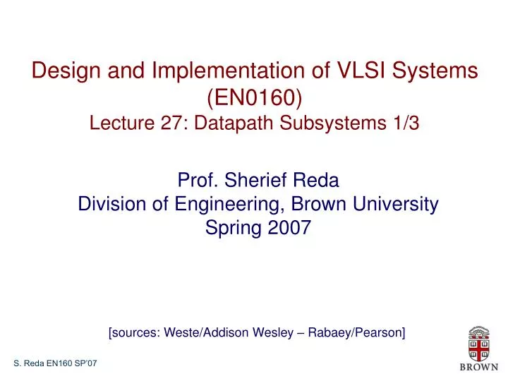
Design and Implementation of VLSI Systems (EN0160) Lecture 27: Datapath Subsystems 1/3. Prof. Sherief Reda Division of Engineering, Brown University Spring 2007. [sources: Weste/Addison Wesley – Rabaey/Pearson].

E N D
Design and Implementation of VLSI Systems (EN0160) Lecture 27: Datapath Subsystems 1/3 Prof. Sherief Reda Division of Engineering, Brown University Spring 2007 [sources: Weste/Addison Wesley – Rabaey/Pearson]
Phase I: Turn your standard cells to Mike today. Mike will iterate with you for the next couple of days and distribute the library file/report on Wednesday April 11. Phase 2: Write precisely the interface (input/output) of your module in the CPU and write in plain english or pseudo-code what your module should do/output for different input combinations. Turn this in to Brian by Monday (April 16). Brian will verify everything and distribute the report on April 18. Project update
Why do we get the “not enough metal density” DRC warning? Downforce Polishing pad Wafer carrier Slurry dispenser Wafer Polishing slurry Rotating platen Area fill features Post-CMP ILD thickness Answer to a FAQ on the standard cell DRC • CMP (chemical mechanical polishing) is executed for each layer before buildup of other layers • How can metal fill insertion helps in smoothing surfaces?
Addition is the most commonly used arithmetic operation It is often the speed limiting element Careful optimization of the adder is of the utmost importance Optimization can be carried out at the circuit or logic level Adders
A N-bit adder can be constructed by cascading 1-bit FA Worst case delay linear with the number of bits td = O(N) tadder = (N-1)tcarry + tsum Goal: Make the fastest possible carry path circuit
Nevertheless Cons • Ci is connected to the transistor closest to the output • Large area • Tall transistor stacks • Large intrinsic capacitance for Co Problems with the design
Even cell Odd cell A B A B A B A B 0 0 1 1 2 2 3 3 C C C C C i ,0 o ,0 o ,1 o ,2 o ,3 FA FA FA FA S S S S 0 1 2 3 Minimize critical path (carry) by reducing the number of inverters , , , , • FA’ does not have an output inverter
For a full adder, define what happens to carry Generate: Cout = 1 independent of C G = A • B Propagate: Cout = C P = A B Kill: Cout = 0 independent of C K = ~A • ~B Can we do better? PGK design