Download
1 / 14
260 likes | 791 Vues
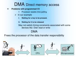
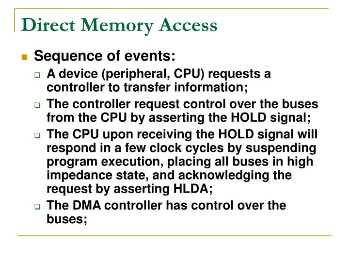
Direct Memory Access. Sequence of events: A device (peripheral, CPU) requests a controller to transfer information; The controller request control over the buses from the CPU by asserting the HOLD signal;

E N D
Direct Memory Access • Sequence of events: • A device (peripheral, CPU) requests a controller to transfer information; • The controller request control over the buses from the CPU by asserting the HOLD signal; • The CPU upon receiving the HOLD signal will respond in a few clock cycles by suspending program execution, placing all buses in high impedance state, and acknowledging the request by asserting HLDA; • The DMA controller has control over the buses;
Direct Memory Access • The DMA controller performs data transfers; • DMA read – transfer from memory to I/O device; • DMA write - transfer from I/O device to memory; • Memory to memory transfers; • When transfers are completed the DMA controller returns control of the buses to the CPU by removing the HOLD signal; • The CPU gains control over the buses and it removes the HLDA signal.
8237 – DMA Controller • Features: • Four Independent Maskable Channels with Autoinitialization Capability; • Cascadable to any Number of Channels • High Speed Data Transfers: • Up to 4MBytes/sec with 8MHz Clock • Up to 6.25MBytes/sec with 12.5MHz Clock • Memory-to-Memory Transfers
8237 – DMA Controller • Static CMOS Design Permits Low Power Operation • ICCSB = 10mA Maximum • ICCOP = 2mA/MHz Maximum • Fully TTL/CMOS Compatible • Internal Registers may be Read from Software
8237 – Pin Definitions • CLK: Clock input. • CS’: Enable for 8237 programming. • RESET: Clears the command, status, request, temporary registers and first/last flip-flop. Sets the mask register. • READY: Logic 0 on READY causes the 8237 to enter wait states for slow memory or I/O device operation. • HLDA: Signal the 8237 that the CPU has relinquished the bus.
8237 – Pin Definitions • DREQ0-DREQ3: DMA request inputs. • DB0-DB7: Data bus. • IOR’: I/O read. • IOW’: I/O write. • EOP’: End of process. • A0-A3: Address lines used to select the internal registers. • HRQ: Hold request. • DACK0-DACK3: DMA channel acknowledge.
8237 – Pin Definitions • AEN: Address enable. • ADSTB: Address strobe. • MEMR’: Memory read. • MEMW’: Memory write.
8237 – Internal registers • The 8237 has several register to be used in its operation. They are listed below. • Current address register - CAR; • Current word count register - CWCR; • Base address register - BA; • Base word count register - BWC; • Command register – CR; • Mode register – MR; • Bus request register – BR; • Mask register set/reset – MRSR; • Mask register – MSR; • Status register – SR.
8237 – Programming • Programming • The 82C37A will accept programming from the host processor anytime that HLDA is inactive, and at least one rising clock edge has occurred after HLDA went low. It is the responsibility of the host to assure that programming and HLDA are mutually exclusive. • Disable the controller (setting bit 2 in the Command register) or masking the channel before programming any of its registers. Once the programming is complete, the controller can be enabled/unmasked. • After power-up it is suggested that all internal locations be loaded with some known value, even if some channels are unused. This will aid in debugging.