Download
1 / 16
1.18k likes | 4.13k Vues
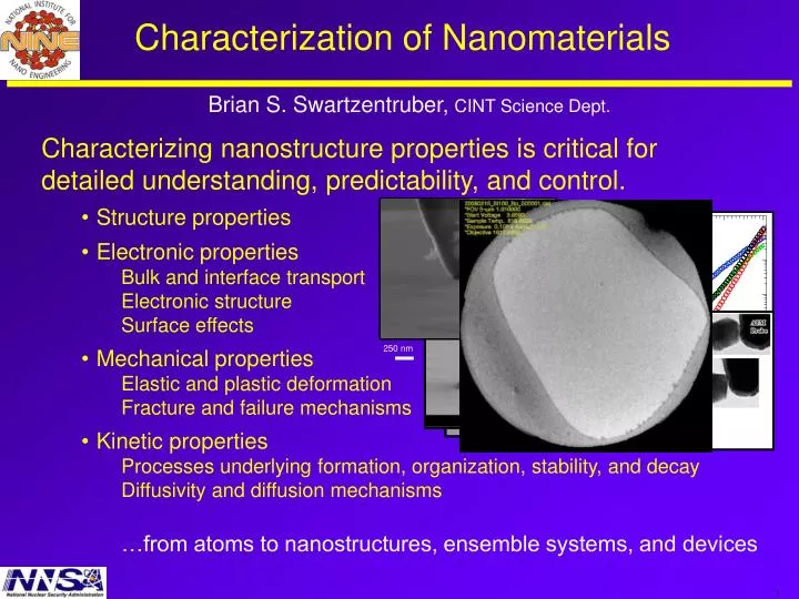
250 nm. Characterization of Nanomaterials. Brian S. Swartzentruber, CINT Science Dept. Characterizing nanostructure properties is critical for detailed understanding, predictability, and control. Structure properties Electronic properties Bulk and interface transport Electronic structure

E N D
250 nm Characterization of Nanomaterials Brian S. Swartzentruber, CINT Science Dept. Characterizing nanostructure properties is critical for detailed understanding, predictability, and control. • Structure properties • Electronic properties Bulk and interface transport Electronic structure Surface effects • Mechanical properties Elastic and plastic deformation Fracture and failure mechanisms • Kinetic properties Processes underlying formation, organization, stability, and decay Diffusivity and diffusion mechanisms …from atoms to nanostructures, ensemble systems, and devices
A meandering localized defect enables the adatom to diffuse via hopover. 1.24 eV Temperature dependence yields the activation barrier. r2 adatom r r1 L STM can probe atom-scale motion directly w/ Ezra Bussmann Brian Swartzentruber, 844-6393 Distinctive features of the statistics of motion – a nonbinomial jump distribution, a nonexponential wait-time distribution, and direction and time correlations – imply 1-d hopover diffusion.
160 nm 250 nm 0 A 4 mm AFM provides rapid characterization of surface nanostructures Julia Hsu, 284-1173 topography current Carbon fiber in insulating polymer matrix Top of zinc oxide nanorods
Conducting AFM enables correlation between topography and conductance electrode topography current 4 mm 4 mm 4 mm w/ Aaron Trionfi Julia Hsu, 284-1173 Investigate percolation transport of carbon nanofiber - polyimide (insulating polymer) composite microscopically using CAFM. Current passes through carbon nanofiber network only (not all nanofibers are part of network).
Piezoelectric force microscopy (PFM) relates mechanical and electrical state of materials 160 nm Topo 250 nm 0 Tip 7 pm/V pA amplifier PFM i Au coat Nanorod Bias voltage Polymer 0 PFM Current The piezoelectric response correlates directly with the resistivity of the nanorods. 500 nm d33 Response (pm/V) Resistivity (Ωcm) w/ David Scrymgeour Julia Hsu, 284-1173 Embedded zinc oxide nanorods
xyz Piezo Controller A complete force profile – approach and retract – for a diamond tip on a NaCl crystal. The tip ‘attaches’ to the salt at DC and, upon retraction, pulls out a nanowire that breaks at DR. Sample Common Plate and Torsion Bars Probe Cantilever AFM behavior Interfacial Force Microscopy (IFM) has a non-compliant force sensor that eliminates “snap-to-contact” w/ Nathan Moore Jack Houston, 844-8939 The force sensor uses two capacitors in a ‘teeter-totter’ configuration to balance the force.
TEM-STM TEM-AFM TEM-Indenter The Tecnai F30 TEM at CINT contains specialized piezo-controlled probes Jianyu Huang, 284-5963 Pulling a nanowire from the NaCl substrate in real time shows the fast diffusion kinetics, defect density, and recrystallization.
TB Magnetic nano-particles can be synthesized and imaged in an air-free environment before transfer for magnetic characterization. The ‘air-free’ TEM allows transfer through a glove-box without contamination Todd Monson, 845-2129
Probe contacts Au catalyst particle for IV measurement through the Ge rod. Rods are rectifying with diameter-dependent behavior. Theoretical ‘carrier-recombination’ mechanism has ideality factor of two. Rods of diameter > 75 nm appear bulk-like. Depletion width increases in smaller rods. Ideality factor Nanomanipulator current-voltage measurements yield metal-semiconductor interface character. Nanomanipulator in an SEM allows electrical characterization and direct manipulation of nanostructures w/ Alec Talin Brian Swartzentruber, 844-6393 Ge rods are grown from Au catalyst in a variety of sizes. Forward-bias exponential slope yields ‘ideality factor’.
250 nm 500 nm Nanomanipulator in an SEM allows electrical characterization and direct manipulation of nanostructures Brian Swartzentruber, 844-6393 Pulling probe from salt crystal plastically deforms outer layer. Joystick positioning and programming command allow precise placement and motion control. Electron beam ‘shadow’ helps position probe. 100 nm GaAs rod Tip-nanostructure adhesion allows pick-and-place. Advantage: complete flexibility in hardware, software, and data acquisition
20 mm gap for sample Thermal driven force actuator Calibrated load measurement electrolyte channel CynthiaVolkert (University of Goettingen, Germany) 2008 CINT User Project seals electrode 1 window electrode 2 Designing micro-scale platforms for testing mechanical, thermal, and electrochemical properties Mechanical Properties Thermal Properties John Sullivan, 845-9496 CINT Cantilever Array Discovery Platform™ • Thermal & electrical properties of nanoscale materials Electrochemical Properties • Real-time imaging of electrochemical processes with nanoscale resolution • Electrochemical cell that operates inside a TEM
Decay of NMR signal as a function of field gradient yields particle diffusivity. Pulsed field gradient nuclear magnetic resonance (PFG-NMR) measures the diffusion of nanoparticles in solution Todd Alam, 844-1225 Self diffusion and molecular motion of liquids in nano-materials can be measured. Details about the impact of morphology on transport properties within nano-composites and the assembly of nanoparticles and dendrimers are determined. Present Sandia investigations include: • Diffusion measurements of H2O within fuel cell membranes. How do changes in membrane nano-morphology (domain size, pore size and surface modification) control the transport rates? • Measurement of transport in porous materials, and impact of nanostructure on transport of different molecular species • Measurement of the interaction and aggregation between surface modified nanoparticles and the impact of diffusion of these assemblies.
Increasing Pb coverage Overlayer white - Alloy black Low-energy electron microscope (LEEM) images of Pb/Cu(111) 4 m 4 m Low-energy electron microscope (LEEM) can image real-time surface nano-structure formation and self-assembly processes Gary Kellogg, 844-2079 Patterns are thermodynamic, arising from stress difference between the two phases. But kinetics have to be fast enough to allow the patterns to form! Pb/Cu(111) • Spatial resolution: 7-8 nm • Time resolution: video rates • Sample temperature: 150 K -1800 K • Background pressure: UHV • Contrast mechanisms: work function differences (surface chemistry, doping differences), electron interference (surface steps), electron diffraction (surface reconstructions), etc. Plass et al.
Schematic of test structure 1000 μm Intensity (arb. units) =1.2 V n-type lines Start Voltage (V) p-type (~1019) Blanket n-type implant (<1017) p-type n-type LEEM images show p-n contrast on device test structures w/ Meredith Anderson Gary Kellogg, 844-2079 LEEM image of p-n interface p-type n-type 10 μm FOV, 0.90 μm line Ramping incident electron energy yields information on surface potential, doping, and oxide properties.
SEM + Nanoprober to arrive fall ‘08 FIB for Imaging and Circuit Editing TIVA Defect Isolation TIVA and STEM for Optoelectronic Failure Analysis Soft Defect Localization (SDL) Microsystems reliability and failure analysis is pushing to the nanoscale David Stein, 845-8476 • Charge-Induced Voltage Alteration (CIVA) • Low Energy CIVA (LECIVA) • Light-Induced Voltage Alteration (LIVA) • Seebeck Effect Imaging (SEI) • Thermally-Induced Voltage Alteration (TIVA) Measure voltage fluctuations in a constant-current power supply as an electron or photon beam is scanned across an IC. • Expertise in Si CMOS, III-V, MEMS, and Optoelectronics • Support throughout the product life cycle • Extensive reliability & failure analysis capabilities, equipment, tools & techniques
Characterizing nanostructure properties is critical for detailed understanding, predictability, and control • STM can probe atom-scale motion directly • AFM provides rapid characterization of surface nanostructures • Conducting AFM enables correlation between topography and conductance • Piezoelectric force microscopy (PFM) relates mechanical and electrical state of materials • Interfacial Force Microscopy (IFM) has a non-compliant force sensor that eliminates “snap-to-contact” • The Tecnai F30 TEM at CINT contains specialized piezo-controlled probes • The ‘air-free’ TEM allows transfer through a glove-box without contamination • Nanomanipulator in an SEM allows electrical characterization and direct manipulation of nanostructures • Designing micro-scale platforms for testing mechanical, thermal, and electrochemical properties • Pulsed field gradient nuclear magnetic resonance (PFG-NMR) measures the diffusion of nanoparticles in solution • Low-energy electron microscope (LEEM) can image real-time surface nano-structure formation and self-assembly processes • LEEM images show p-n contrast on device test structures • Microsystems reliability and failure analysis is pushing to the nanoscale Brian Swartzentruber, 844-6393 Julia Hsu, 284-1173 Julia Hsu, 284-1173 Julia Hsu, 284-1173 Jack Houston, 844-8939 Jianyu Huang, 284-5963 Todd Monson, 845-2129 Brian Swartzentruber, 844-6393 John Sullivan, 845-9496 Todd Alam, 844-1225 Gary Kellogg, 844-2079 Gary Kellogg, 844-2079 David Stein, 845-8476 Contact information is on the poster.