Download
1 / 76
780 likes | 935 Vues
Lecture 42: Review of active MOSFET circuits. Prof. J. S. Smith. Final Exam. Covers the course from the beginning Date/Time: SATURDAY, MAY 15, 2004 8-11A Location: BECHTEL auditorium One page (Two sides) of notes. Observed Behavior: I D - V DS.

E N D
Lecture 42: Review of active MOSFET circuits Prof. J. S. Smith
Final Exam • Covers the course from the beginning • Date/Time: SATURDAY, MAY 15, 2004 8-11A • Location: BECHTEL auditorium • One page (Two sides) of notes University of California, Berkeley
Observed Behavior: ID-VDS • For low values of drain voltage, the device is like a resistor • As the voltage is increases, the resistance behaves non-linearly and the rate of increase of current slows • Eventually the current stops growing and remains essentially constant (current source) non-linear resistor region “constant” current resistor region University of California, Berkeley
Observed Behavior: ID-VDS non-linear resistor region “constant” current resistor region As the drain voltage increases, the E field across the oxide at the drain end is reduced, and so the charge is less, and the current no longer increases proportionally. As the gate-source voltage is increased, this happens at higher and higher drain voltages. The start of the saturation region is shaped like a parabola University of California, Berkeley
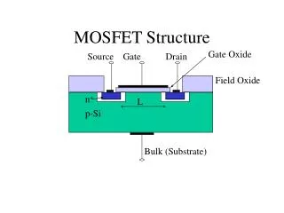
Finding ID = f (VGS, VDS) • Approximate inversion charge QN(y): drain is higher than the source less charge at drain end of channel University of California, Berkeley
Inversion Charge at Source/Drain The charge under the gate along the gate, but we are going to make a simple approximation, that the average charge is the average of the charge near the source and drain University of California, Berkeley
Average Inversion Charge Drain End Source End • Charge at drain end is lower since field is lower • Notice that this only works if the gate is inverted along its entire length • If there is an inversion along the entire gate, it works well because Q is proportional to V everywhere the gate is inverted University of California, Berkeley
Drift Velocity and Drain Current “Long-channel” assumption: use mobility to find v And now the current is just charge per area, times velocity, times the width: Inverted Parabolas University of California, Berkeley
Square-Law Characteristics Boundary: what is ID,SAT? TRIODE REGION SATURATION REGION University of California, Berkeley
The Saturation Region When VDS > VGS – VTn, there isn’t any inversion charge at the drain … according to our simplistic model Why do curves flatten out? University of California, Berkeley
Square-Law Current in Saturation Current stays at maximum (where VDS = VGS – VTn ) Measurement: ID increases slightly with increasing VDS model with linear “fudge factor” University of California, Berkeley
A Simple Circuit: An MOS Amplifier Input signal Supply “Rail” Output signal University of California, Berkeley
Small Signal Analysis • Step 1: Find DC operating point. Calculate (estimate) the DC voltages and currents (ignore small signals sources) • Substitute the small-signal model of the MOSFET/BJT/Diode and the small-signal models of the other circuit elements. • Solve for desired parameters (gain, input impedance, …) University of California, Berkeley
Supply “Rail” A Simple Circuit: An MOS Amplifier Input signal Output signal University of California, Berkeley
VGS,BIAS was found in Lecture 15 Small-Signal Analysis Step 1. Find DC Bias – ignore small-signal source IGS,Q University of California, Berkeley
Small-Signal Modeling What are the small-signal models of the DC supplies? Shorts! University of California, Berkeley
Small-Signal Models of Ideal Supplies Small-signal model: short open University of California, Berkeley
Small-Signal Circuit for Amplifier University of California, Berkeley
Low-Frequency Voltage Gain Consider first 0 case … capacitors are open-circuits Design Variable Transconductance Design Variables University of California, Berkeley
Voltage Gain (Cont.) Substitute transconductance: Output resistance: typical value n= 0.05 V-1 Voltage gain: University of California, Berkeley
Input and Output Waveforms Output small-signal voltage amplitude: 14 x 25 mV = 350 Input small-signal voltage amplitude: 25 mV University of California, Berkeley
What Limits the Output Amplitude? 1. vOUT(t) reaches VSUP or 0… or 2. MOSFET leaves constant-current region and enters triode region University of California, Berkeley
Maximum Output Amplitude vout(t)= -2.18 V cos(t) vs(t) = 152 mV cos(t) How accurate is the small-signal (linear) model? Significant error in neglecting third term in expansion of iD= iD(vGS) University of California, Berkeley
One-Port Models (EECS 40) • A terminal pair across which a voltage and associated current are defined Circuit Block University of California, Berkeley
Small-Signal Two-Port Models • We assume that input port is linear and that the amplifier is unilateral: • Output depends on input but input is independent of output. • Output port : depends linearly on the current and voltage at the input and output ports • Unilateral assumption is good as long as “overlap” capacitance is small (MOS) University of California, Berkeley
Two-Port Small-Signal Amplifiers Voltage Amplifier Current Amplifier University of California, Berkeley
Two-Port Small-Signal Amplifiers Transconductance Amplifier Transresistance Amplifier University of California, Berkeley
Common-Source Amplifier (again) How to isolate DC level? University of California, Berkeley
DC Bias 5 V Neglect all AC signals 2.5 V Choose IBIAS, W/L University of California, Berkeley
Load-Line Analysis to find Q Q University of California, Berkeley
Small-Signal Analysis University of California, Berkeley
Two-Port Parameters: Generic Transconductance Amp Find Rin, Rout, Gm University of California, Berkeley
Two-Port CS Model Reattach source and load one-ports: University of California, Berkeley
Maximize Gain of CS Amp • Increase the gm (more current) • Increase RD (free? Don’t need to dissipate extra power) • Limit: Must keep the device in saturation • For a fixed current, the load resistor can only be chosen so large • To have good swing we’d also like to avoid getting too close to saturation University of California, Berkeley
Current Source Supply • Solution: Use a current source! • Current independent of voltage for ideal source University of California, Berkeley
CS Amp with Current Source Supply University of California, Berkeley
Load Line for DC Biasing Both the I-source and the transistor are idealized for DC bias analysis University of California, Berkeley
Two-Port Parameters From current source supply University of California, Berkeley
P-Channel CS Amplifier DC bias: VSG = VDD – VBIAS sets drain current –IDp = ISUP University of California, Berkeley
Common Gate Amplifier Notice that IOUT must equal -Is DC bias: Gain of transistor tends to hold this node at ss ground: low input impedance load for current input current gain=1 Impedance buffer University of California, Berkeley
CG as a Current Amplifier: Find Ai University of California, Berkeley
CG Input Resistance At input: Output voltage: University of California, Berkeley
Approximations… • We have this messy result • But we don’t need that much precision. Let’s start approximating: University of California, Berkeley
CG Output Resistance University of California, Berkeley
CG Output Resistance Substituting vs= itRS The output resistance is (vt / it)|| roc University of California, Berkeley
Approximating the CG Rout The exact result is complicated, so let’s try to make it simpler: Assuming the source resistance is less than ro, University of California, Berkeley
CG Two-Port Model Function: a current buffer • Low Input Impedance • High Output Impedance University of California, Berkeley
Common-Drain Amplifier In the common drain amp, the output is taken from a terminal of which the current is a sensitive function Weak IDS dependence University of California, Berkeley
CD Voltage Gain Note vgs = vt – vout University of California, Berkeley