Download
1 / 14
190 likes | 443 Vues
MOSFET V-I Characteristics. Vijaylakshmi.B Lecturer, Dept of Instrumentation Tech Basaveswar Engg. College Bagalkot, Karnataka. IUCEE-VLSI Design, Infosys, Mysore. Types of Transistors. n-channel. p-channel. n-channel. p-channel. Depletion type. Enhancement type. MOSFET (Types).

E N D
MOSFET V-I Characteristics Vijaylakshmi.B Lecturer, Dept of Instrumentation Tech Basaveswar Engg. College Bagalkot, Karnataka IUCEE-VLSI Design, Infosys, Mysore
n-channel p-channel n-channel p-channel Depletion type Enhancement type MOSFET (Types) • Four types: • n-channel enhancement mode • Most common since it is cheapest to manufacture • p-channel enhancement mode • n-channel depletion mode • p-channel depletion mode
MOSFET FET = Field-Effect Transistor A four terminal device (gate, source, drain, bulk) Symbols of MOSFET
MOSFET characteristics • Basically low voltage device. High voltage device are available up to 600V but with limited current. Can be paralleled quite easily for higher current capability. • Internal (dynamic) resistance between drain and source during on state, RDS(ON), , limits the power handling capability of MOSFET. High losses especially for high voltage device due to RDS(ON) . • Dominant in high frequency application (>100kHz). Biggest application is in switched-mode power supplies.
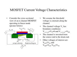
The transistor consists of three regions, labeled the ``source'', the ``gate'' and the ``drain''. • The area labeled as the gate region is actually a ``sandwich'' consisting of the underlying substrate material, which is a single crystal of semiconductor material (usually silicon); a thin insulating layer (usually silicon dioxide); and an upper metal layer. • Electrical charge, or current, can flow from the source to the drain depending on the charge applied to the gate region. • The semiconductor material in the source and drain region are ``doped'' with a different type of material than in the region under the gate, so an NPN or PNP type structure exists between the source and drain region of a MOSFET.
Most important device in digital design • Very good as a switch • Relatively few parasitics • Rather low power consumption • High integration density • Simple manufacturing • Economical for large complex circuits
NMOS Structure • MOS (Metal-Oxide-Semiconductor) Nowadays gate is made of poly-silicon Channel length L and width W In most digital design, L is set at the minimum feature size W is selectable by the designer Bulk is connected to the Gnd in NMOS to prevent forward-biased PN junction Off state On state
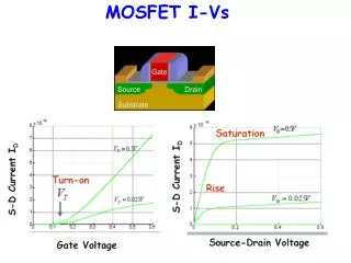
n-MOSFET Characteristics Plots V-I characteristics of the device for various Gate voltages (VGS) At a constant value of VDS , we can also see that IDS is a function of the Gate voltage, VGS The transistor begins to conduct when the Gate voltage, VGS , reaches the Threshold voltage: VT
PMOS Structure • PMOS transistor has a negative threshold voltage (Vtp) -0.3v~-1.2v • A pMOS turns on when Vgs<Vtp
P-MOSFET Characteristics The terminal characteristics of the device are given by drain-to-source current Ids against drain-to-source voltage Vds for different values of gate-to-source voltage Vgs. All voltages are referenced with respect to the source voltage, which is assumed to be at ground potential.