Download
1 / 16
160 likes | 315 Vues
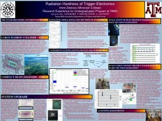
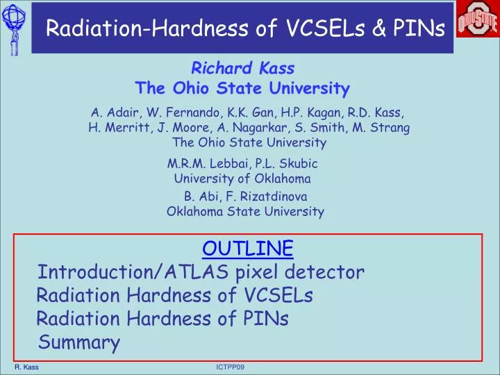
Richard Kass The Ohio State University. Radiation-Hardness of VCSELs & PINs. A. Adair, W. Fernando, K.K. Gan, H.P. Kagan, R.D. Kass, H. Merritt, J. Moore, A. Nagarkar, S. Smith, M. Strang The Ohio State University. M.R.M. Lebbai, P.L. Skubic University of Oklahoma. B. Abi, F. Rizatdinova

E N D
Richard Kass The Ohio State University Radiation-Hardness of VCSELs & PINs A. Adair, W. Fernando, K.K. Gan, H.P. Kagan, R.D. Kass, H. Merritt, J. Moore, A. Nagarkar, S. Smith, M. Strang The Ohio State University M.R.M. Lebbai, P.L. Skubic University of Oklahoma B. Abi, F. Rizatdinova Oklahoma State University OUTLINE Introduction/ATLAS pixel detector Radiation Hardness of VCSELs Radiation Hardness of PINs Summary
~1.85m The Current ATLAS Pixel Detector ATLAS: an LHC detector designed to study 14 TeV pp collisions Pixel detector is inner-most system -> Radiation damage is the issue Present Pixel Detector: ATLAS’s Inner most charged particle tracker Measures (x,y,z) to ~30 mm Pixel detector is based on silicon Pixel size 50mm by 400 mm ~80 million pixels Radiation hardness is an issue must last ~ 10 years A pixel module contains: 1 sensor (2x6cm) ~40000 pixels 16 front end (FE) chips 2x8 array Flex-hybrid 1 module control chip (MCC) There are ~1744 modules Detector upgrades planned: New Inner layer (“IBL”) & later a new pixel detector for Super-LHC
Present Pixel Opto-link Architecture Current optical link of pixel detector transmits signals at 80 Mb/s Opto-link separated from FE modules by ~1m transmit control & data signals (LVDS) to/from modules on micro twisted pairs Use PIN/VCSEL arrays Use 8 m of rad-hard/low-bandwidth SIMM fiber fusion spliced to 70 m rad-tolerant/medium-bandwidth GRIN fiber a Simplify opto-board and FE module production a Sensitive optical components see lower radiation level than modules a PIN/VCSEL arrays allow use of robust ribbon fiber ~80m ~1m optoboard VCSEL:Vertical Cavity Surface Emitting Laser diode VDC:VCSEL Driver Circuit PIN:PiNdiode DORIC:Digital Optical Receiver Integrated Circuit optoboard holds VCSELs, VDCs, PINS
Radiation Dosage at SLHC VCSEL/PIN of current pixel detector are mounted on patch panel (PP0) instead of directly on the pixel module a much reduced radiation level compared with module VCSEL/PIN for pixel detector at SLHC will be mounted further away from pixel module aexpected dosage at r = 37 cm for 3,000 fb-1 with 50% safety factor: usilicon: 7.2 x 10¹⁴ 1-MeV neq/cm2 uGaAs: 2.8 x 10¹⁵ 1-MeV neq/cm2 Assuming radiation damage scales with Non-Ionizing Energy Loss (NIEL)
Real Time Monitoring in T7 Beam Test 24 GeV proton beam 2009 Beam Tests used a simple system Real time monitoring of PIN current & optical power. VCSEL arrays laser spot = beam spot Control Room PIN diode arrays VCSEL arrays
850 nm VCSEL Irradiation 2006-7: 12-channel VCSEL arrays were irradiated to SLHC dosage AOC 2.5 Gb/s (obsolete), 5 Gb/s, 10 Gb/s ULM 5 Gb/s, 10 Gb/s Optowell 2.5 Gb/s insufficient time for annealing during irradiation 2008: AOC 5 Gb/s, 10 Gb/s Optowell 2.5 Gb/s 2009: AOC 10 Gb/s goal: 20 arrays actual: 6 arrays due to manufacturer problem MPO connector MPO adaptor Opto-pack
irradiation annealing 7.6 x 10¹⁵ 1-MeV neq/cm2 AOC 10 Gb/s VCSEL (2008) Optical power recovery by annealing is slow Almost recover the initial power after extended annealing VCSEL produces more power at lower temperature
AOC 10 Gb/s VCSEL (2009) irradiation annealing 4.4 x 10¹⁵ 1-MeV neq/cm2 w/o long twisted/coiled fiber 145 mW Good optical power for 6 arrays irradiated Await return of arrays to OSU for annealing/characterization need to irradiate a sample of 20 arrays in 2010
2008 PIN Irradiation Irradiated 2 arrays or several single channel devices of each type Hamamatsu devices: low bandwidth but more radiation hard Irradiated 20 Optowell arrays in 2009
PIN Responsivity vs Bias Voltage (2008) 4.4 x 10¹⁵ 1-MeV neq/cm2 Pre-irrad Optowell Optowell AOC ULM Responsivity doesn’t depend on bias voltage before irradiation Can increase responsivity with higher bias after radiation
PIN Responsivity vs Bias Voltage Optowell Can fully recover pre-irradiation responsivity with large bias voltage Need to look at pulse shape at high bias voltage
Optowell Eye Diagram at High Bias Voltage Test limited to 1 Gb/s @ 40 V due to carrier board limitation Eye diagram looks reasonable aneed more detailed characterization
10 arrays 60 Pre-Irrad Post-Irrad 50 40 Channels 30 20 10 0 0.1 0.2 0.3 0.4 0.5 0.6 0.7 0.8 Responsivity (A/W) Results on Optowell PIN Arrays 20 Optowell PIN arrays irradiated August 2009 Good responsivity after irradiation average responsivity after irradiation ~0.3 A/W Analysis of additional ten arrays complicated by beam misalignment Need more detailed study, including eye diagram after cool down. 8.1 x 10¹⁵ 1-MeV neq/cm2
Summary AOC 10 Gb/s arrays have good optical power after irradiation VCSEL produces more power as room temperature decreases Need to repeat irradiation with large sample in 2010 Hamamatsu PINs are slow but more radiation hard Optowell PIN arrays have good responsivity after irradiation Can increase responsivity with higher bias voltage after radiation Will irradiate a large sample of AOC PIN arrays in 2010 AOC plans to release high-speed PIN arrays in 2010
Opto-board clock PIN DORIC data VDC VCSEL VCSEL VDC Real Time Monitoring in T7 Beam Test Compare transmitted and decoded data Measure minimum PIN current for no bit errors Measure optical power Signal routed back to opto-baord via test board attached to 80-pin connector & test board 2006-8 test of opto-board system used loop-back setup 25m optical fiber cable bi-phase marked optical signal Opto-Chip setup decoded data decoded clock In beam In control room Bit error test setup at CERN’sT-7 beamline 24 GeV protons Two VCSEL arrays from same vendor per opto-board