Download
1 / 46
680 likes | 1.14k Vues
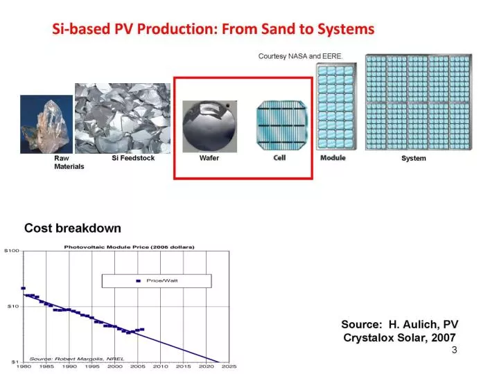
Solar Cell Production. Silicon dioxide to Polysilicon. Silicon dioxide Carbon-arc reduction furnace Metallurgical silicon Purification Chlorination and distillation Deposition furnace Decomposition into solar grade polysilicon. Polysilicon to Ingots. Crucible Furnace 1500ºC

E N D
Silicon dioxide to Polysilicon Silicon dioxide Carbon-arc reduction furnace Metallurgical silicon Purification Chlorination and distillation Deposition furnace Decomposition into solar grade polysilicon
Polysilicon to Ingots Crucible Furnace 1500ºC Crystalizationinto a solid state Cooling from the base up Rising of the few remaining impurities to the top Multicrystallineingot of extremely pure silicon
Ingots to Wafers Cut into smaller bricks High-precision wire saws Cut into very thin slices, known as 'wafers‘ The thickness of the wafer as low as one fifth of a millimeter.
Wafers to Cells An alkaline solution: To smooth away any damage the wire saws may have caused Etching of the outer face: To give the surface a texture to increase the level of sunlight absorbed A dopant element: In order to alter the optical/electrical properties of the semiconductor Thin layer of anti-reflecting material: To maximize light absorption Screen-printing: To add electrical contacts
Cells to Modules Solar cells are the heart of solar modules. The cells are connected into strings that are then encapsulated in polymers under glass. Modules can produce up to 500 watts and manage up to 1000 volts
Modules to Systems Modules are the sections of a solar system. A system can be just one module, or thousands. Systems are tailored to meet specific needs, with variations such as battery storage to provide AC or DC power, inverters, connectors and power controls.
Phosphosilicate Glass Etch • During the phosphorus predep a layer of phosphosilicate glass was grown on the surface of the silicon. This layer will act as a constant source of dopants for subsequent diffusion steps, thus fixing the surface concentration of the phosphorus doped areas to the solid solubility limit.
In order to remove the PSG • A three step etch: Remove PSG: HF etchchemical Oxidation:H2SO4/HNO3remove chemically Oxidized layer:HF etch
why In-line Diffusion? Formation of the pn-junction by phosphorus diffusion is one critical part of the manufacturing process for crystalline silicon solar cells, which affects performance and cost of the product. So far diffusion in tube furnaces with POCl3 is the dominant principle. The process is well understood and has proven performance on industrial scale. However, because it is a batch process, POCl3 diffusion requires complex handling with the risk of wafer breakage and cost of ownership is high. Therefore, there is a demand for alternatives and inline diffusion attracts attention.
In-line Diffusion Consist of two steps: 1- coating of the wafers with a phosphorus containing dopant 2- diffusion of the phosphorus from the dopant into the silicon in an inline furnace. A common approach to coat the wafers is spraying of the dopant. A drawback of this method is the need for adding surfactants or organic solvents to achieve good wetting and thus homogeneous coating. These additives disturb the diffusion process and increase it complexity and cost.
A textured cell without the anti-reflection coating will appear gray. With the coating, it will appear black or close to black.
Why solar cells are sometimes blue • These are untextured silicon solar cells with a layer of silicon nitride anti-reflection coating on top. They appear blue because the anti-reflection coating is optimized for a certain wavelength of the solar spectrum. They are most likely poly-silicon cells because it has been difficult to texture the front surface of polysilicon (the crystal grains aren't all aligned in the same direction).
It is easier to texture monocrystalline silicon because it is a single crystal grain. Just dip it in KOH for some amount of time and the anisotropic etching process will produce random pyramids on the surface. If a company for some reason decides not to texture a monocrystalline silicon cell or improperly texture it, it will also appear blue. With recent advances in acid etching, however, texturing polysilicon will become more mainstream, and you might not see blue cells off the line anymore.
Reactive Ion Etching (RIE) Etching • A disadvantage of wet etching is the undercutting caused by the isotropy of the etch. The purpose of dry etching is to create an anisotropic etch - meaning that the etch is uni-directional. • An anisotropic etch is critical for high-fidelity pattern transfer. • RIE etching is one method of dry etching. • An RIE consists of two electrodes (1 and 4) that create an electric field (3) meant to accelerate ions (2) toward the surface of the samples (5). • The area labeled (2) represents plasma that contains both positively and negatively charged ions in equal quantities. These ions are generated from the gas that is pumped into the chamber. • O2 and CF4 gasses are used for etches. In the Diagram CF4 has been pumped into the chamber, making a plasma with many Fluorine (F-) Ions
Reactive Ion Etching (RIE) Etching • The Fluorine ions are accelerated in the electric field. cause them to collide into the surface of the sample. A hard mask is used to protect certain areas from etching, exposing only the areas desired to be etched. • The figure below shows a photoresist mask on silicon dioxide. The etching ions are accelerated into the etching region, where they combine with silicon dioxide and then are dispersed. Because the electric field accelerated ions toward the surface, the etching caused by these ions is much more dominant than the etching of radicals - ions traveling in varied directions, so the etching is anisotropic.
RPS etch Remote Plasma Source • It generates plasma in a remote chamber. • The etchant gases are allowed to flow through the plasma chamber and dissociate into the plasma, and the free radicals are allowed to flow to the process chamber to react with and etch the materials on the wafer
Solar module manufacturing process • Step 1 : Test & Sort Solar Cells Test and sort solar cells for optimized module performance. Cells of many types and shapes can be used in Spire manufacturing equipment.
Sorts PV cells according to electrical performance Automated cell handling gently positions each cell for electrical testing under simulated sunlight Tested cells are sorted into output bins according to the cell’s electrical performance.
Step 2 :: Tab & String Solar Cells • Interconnect solar cells by soldering flat metal leads, or tabs, to cell contacts, producing solar cell strings.
Step 3 :: Transfer Cell Strings onto Modules • Gently pick up and transfer interconnected solar cells, or strings, from storage trays onto module substrates, accurately aligning the strings to ensure module quality.
Step 4 :: Laminate Solar Modules • Encapsulate solar modules with controlled heat, vacuum and pressure to form a uniform, environmentally-stable, composite structure.
Step 5 :: Trim, Frame & Finish Module Assembly • Trim solar modules after lamination, install edge sealant and structural frames, and attach electrical junction boxes. Mount frames to seal the edges and add structure.
Step 6 :: Test Module Performance • Test the electrical performance of photovoltaic modules under simulated sunlight conditions.