Download
1 / 25
260 likes | 429 Vues
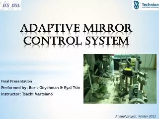
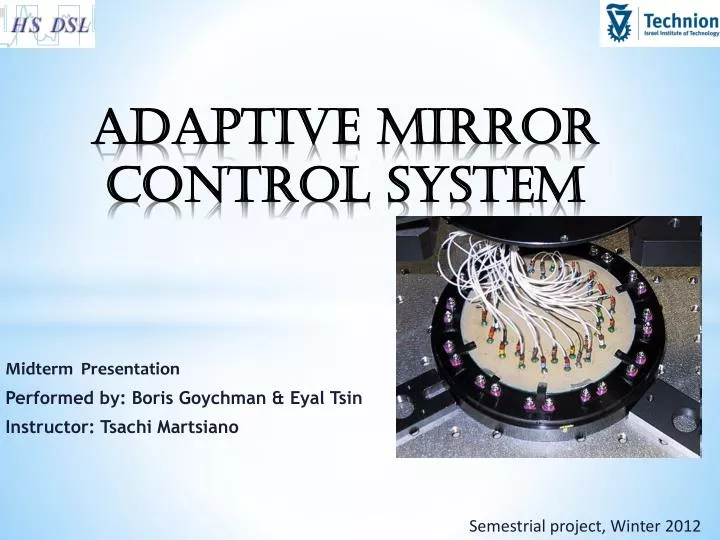
Adaptive Mirror Control System. Midterm Presentation Performed by: Boris Goychman & Eyal Tsin Instructor: Tsachi Martsiano. Semestrial project, Winter 2012. Joint project with physics faculty, deals with an adaptive mirror

E N D
Adaptive Mirror Control System Midterm Presentation Performed by: Boris Goychman& EyalTsin Instructor: TsachiMartsiano Semestrial project, Winter 2012
Joint project with physics faculty, deals with an adaptive mirror • The mirror changes Convexity in order to correct distortions of light originated in the atmosphere • Such mirrors are used with telescopes Background
Building a system that interface with a PC from one end and control an adaptive mirror on the other end. *Adaptive Mirror – contains 126 capacitors to control the shape of the mirror • Learn an approach for practical engineering. • Get familiar with FPGA, Logic Design and board design basics. Projects Goals
D/A Functional description
Microprocessor • Philips provide software and drivers, easy to implement • Need to buy one + external RAM • Board design • FPGA design • Predesigned board • Difficult to test and design with VHDL • Choosing alternative USB control - FTDI • Simple interface • Slower rate (1Mbps) Development alternatives
VHDL implementation • At least 5 FSM’s (1 ready 4 in work) • D/A chip connected (works) • Only 1 Due to area, cost saving reasons • FPGA implementation selected • Due to availability • ISP1362 – USB controller • Used as a device • Initialized with PIO (only way) • Memory data transfer with DMA mode (faster way) Devised solutions
Control a 126 capacitor adaptive mirror • 256 voltage values for each capacitor • Same controller can be used to control any other system with the same requirements • 126 inputs or less • 256 values per input • 1ms refresh rate • The output of the D2A will pass through • a SAMPLE & HOLD (not in the scope of our project) • and then to the mirror (not in the scope of our project) System usage & possible expansions
PC DE2 GUI FPGA Main State Machine D/A controller Memory USB controller Philips USB controller USB General Block Diagram D/A ( Sample and Hold )
D/A PC DE2 FPGA ISP 8 GUI 7 4 S&H S&H S&H S&H General Block Diagram USB 6 16
USB Controller RAM D/A Controller MAIN FPGA
FPGA D/A Manager D/A Controller D/A Control Block
State 1 State 2 State 3 State 0 State 6 State 7 D/A state machine State 4 State 5
State 1a State 2a SW0 SW0 State 2 State R SW0 State 1 SW0 SW0 KEY0 FINISH FINISH SW0 KEY1 State 0 SW0 State 4 State 3 SW0 SW0 SW0 FINISH FINISH State 4a State 3a KEY3 KEY2 D/A emulation state machine
Bin = 0101001 • Dec = 81 Vth = (5*81*1)/256 = 1.582v Vr = 1.572v • Bin = 00110011 • Dec = 51 Vth = (5*51*1)/256 = 0.996v Vr = 0.977v • Bin = 10010000 • Dec = 144 Vth = (5*144*1)/256 = 2.812v Vr = 2.796v D/A Outputs – Theory VS Real Values
FPGA USB CONTROLLER ISP 1363 MANAGER (main program) USB controller Block Diagram RAM 16 16
DMA write/read burst state machine I/O write/read single cycle state machine Look Up Table for initialization process DMA counter I/O counter Main USB controller – state machine USB controller state machine Main counter
A Single Write Cycle A Single Write Cycle • Remarks : • A0 = ADDRESS = 1 / 0 • A1 = 1 • DATA = D = Address / Data to be written / read
Designed the entire system • Connected the D\A component to the DE2 • Encoded the D\A controller and Simulated it in Quartus • Emulated the D\A controller • Read About the USB in general and about the ISP1362 In Particular • Designed the USB’s FSMs • Started to work on the encoding of the USB controller • Started to work on the GUI What we have done so far