Download
1 / 10
110 likes | 402 Vues
ECL Design Laboratory. John Jakabosky – EECS 713. Goals & Deliverables. Design an ECL laboratory exercise to give a participant an understanding of the operating principles of ECL Simulate the operation of the differential current amplifier at the core of the ECL OR/NOR gate

E N D
ECL Design Laboratory John Jakabosky – EECS 713
Goals & Deliverables • Design an ECL laboratory exercise to give a participant an understanding of the operating principles of ECL • Simulate the operation of the differential current amplifier at the core of the ECL OR/NOR gate • Give participant pre and post-lab work to facilitate understanding
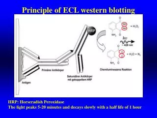
ECL Refresher • ECL is a form of logic that uses npn BJTs • At the core of the design is a differential current amplifier • Trades high static power consumption for fast operation • Outputs must be terminated • Power supplies use negative voltages • Produces less EMI and is more secure (from cryptographic side-channel attacks)
Differential Amplifier • Two N type transistors with coupled emitters • All current is shared between I1 and I2 • v2 is a reference voltage if v1 > v2 then current I2 is small and vout is higher • Otherwise vout is high • The opposite effect is seen on I1 path • Easily exploited to provide OR/NOR logic
Pre-lab work • Recommend watching NPTEL youtube Lecture 18 on Basic ECL Operation http://www.youtube.com/watch?v=MqidrO1TPvQ • Intro video provides • Study the example schematic to be implemented
Lab Assignment • Use PSPICE NPN Q breakout transistor model, set forward β=25 • Design a PSPICE schematic based on the one provided • Use 4mA current source, 250 ohm amplifier resistors • -1.3 V reference, -5.2 V for VEE, 50 ohm input termination • Determine current flow through R4 and R7 for a range of input voltages to 1 transistor input • Set one input transistor to logic low (to demonstrate OR/NOR) • sweep input voltage from -5.2V to 0V • Provide PSPICE simulated current values
Post-Lab Work • Determine power consumption estimate of differential amplifier resistors and BJTs • Questions for participant • Could additional transistors be used to convert current amplifier to output stage? Yes, one additional BJT for each output • At what input voltage does the current flip from one path to the other? 1.3V or VREF • Why is there a reduction in current flow at higher input voltages? The BJT have been forced into saturation • Why might this design be faster than CMOS? Low input/output capacitance
References • http://www.youtube.com/watch?v=MqidrO1TPvQ • http://www.youtube.com/watch?v=BV-2gxFuAH0 • http://en.wikipedia.org/wiki/File:ECL.svg • http://en.wikibooks.org/wiki/Circuit_Idea/Revealing_the_Truth_about_ECL_Circuits • http://www.engr.colostate.edu/ECE562/Pspicetutorial.pdf • http://www.ece.mcmaster.ca/faculty/bakr/ece2ei5/PSpice_Experiment.pdf • http://www.st-andrews.ac.uk/~www_pa/Scots_Guide/audio/part1/page3.html • http://johncohn.org/base/2012/10/11/thursday-morning-history-of-computing/
Questions? Discrete ECL board from IBM Console