Download
1 / 9
120 likes | 349 Vues
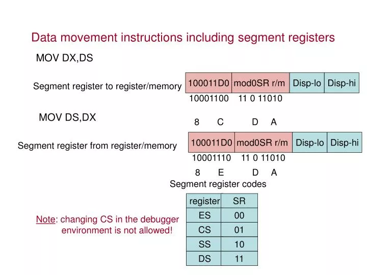
MOV DX,DS. 100011D0. mod0SR r/m. Disp-lo. Disp-hi. Segment register to register/memory. 10001100. 11 0 11010. 8 C D A. Segment register codes. register. SR. ES. 00. Note : changing CS in the debugger environment is not allowed!. CS. 01. SS. 10.

E N D
MOV DX,DS 100011D0 mod0SR r/m Disp-lo Disp-hi Segment register to register/memory 10001100 11 0 11010 8 C D A Segment register codes register SR ES 00 Note: changing CS in the debugger environment is not allowed! CS 01 SS 10 DS 11 Data movement instructions including segment registers MOV DS,DX 100011D0 mod0SR r/m Disp-lo Disp-hi Segment register from register/memory 10001110 11 0 11010 8 E D A
MOV [BP] [DI] +1234,ES 100011D0 mod0SR r/m Disp-lo Disp-hi Segment register to register/memory 10001100 10 0 00011 8 C 8 3 34 12 MOV ES , [BP] [DI] +1234 100011D0 mod0SR r/m Disp-lo Disp-hi Segment register from register/memory 10001110 10 0 00011 8 E 8 3 34 12
1000011W Mod reg r/m Displ-lo Displ-hi More data movement instructions XCHG [D], [S] exchange [D] [S] 100001DW Mod REG r/m XCHG AX, BX 10000111 11 000 011 87 C3 D S XCHG register/memory with register Acc R R Acc R R 10000111 00000110 00110100 00010010 M R 87 06 34 12 R M XCHG AX, [1234]
More data movement instructions XLAT source table translate Operation [[DS]:[[AL]+[BX]]] AL XCHG 1234, BX XLAT translate byte to AL 11010111 D7 This instruction is used to implement look-up tables
Binary Gray 0 0 0 0 0 0 0 0 0 0 0 0 0 0 1 0 0 1 0 0 1 0 0 1 0 1 1 0 1 1 0 1 0 0 1 0 0 1 1 0 1 1 0 1 0 0 1 0 1 0 0 1 1 0 1 1 1 1 0 0 1 0 1 1 1 0 1 1 1 1 0 1 1 0 0 1 0 1 1 1 0 1 1 0 1 0 0 1 1 1 1 1 1 1 0 1 Gray Binary
More data movement instructions Format LEA R16, [datum]load register with datum [R16] is any 16 bit register except segment registers & IP datum is treated as immediate datum!!! Or indirect load LEA R16, [BX] LEA R16, [BP] LEA R16, [SI] LEA R16, [DI] Load R16 with the contents of the specified register
LEA SI, [0200] Load 0200 to register 10001101 Mod reg r/m Disp-lo Disp-hi 10001101 00110110 00000000 00000010 8 D 3 6 00 02 μP μP IP 0100 IP 0104 CS 150A CS 150A DS DS 150A 150A SI XXXX SI 0200 AX AX BX BX
LDS SI, [0200] 11000101 Mod reg r/m Disp-lo Disp-hi 11000101 00110110 00000000 00000010 C 5 3 6 00 02 151A0 C5 151A0 C5 μP μP 151A1 36 IP 0100 IP 0104 151A1 36 151A2 00 151A2 00 CS 150A CS 150A 151A3 02 151A3 02 DS DS 150A 7856 15200 12 152A0 12 SI XXXX SI 3412 34 152A1 34 152A1 152A2 56 AX AX 152A2 56 152A3 78 BX 152A3 BX 78 Format LDS R16, m load register with [DS:m] and DS with [DS:m+2]
Format LES R16, m load register with [DS:m] and ES with [DS:m+2] LES SI, [0200] 11000100 Mod reg r/m Disp-lo Disp-hi 11000100 00110110 00000000 00000010 C 4 3 6 00 02 11100 C5 11100 C5 μP μP 11101 36 IP 0100 IP 0104 11101 36 11102 00 11102 00 CS 1100 CS 1100 11103 02 11103 02 DS DS 1200 1200 12200 12 12200 12 SI XXXX SI 3412 34 12201 34 12201 ES 7856 12202 56 ES 12202 56 12203 78 12203 BX 78